Cold atom system with atom chip wall

a technology of atom chip and vacuum system, which is applied in the field of vacuum cells, can solve the problems of small size and weight, viewport, and inability to allow large optical access, and achieve the effect of simplifying the vacuum system, facilitating maintenance, and facilitating ultra-high vacuum

Active Publication Date: 2006-10-24
COLDQUANTA
View PDF6 Cites 39 Cited by
  • Summary
  • Abstract
  • Description
  • Claims
  • Application Information

AI Technical Summary

Benefits of technology

[0009]The cold-atom cell of the invention provides for several advantages. Firstly, the cold-atom cell can have a small size and lightweight. With both of the standard techniques, the vacuum chamber is much larger than would be required for the function of the atom chip itself. Sealing the chip to a glass cell dramatically reduces the size.
[0011]Thirdly, the invention reduces or eliminates the need for in-vacuum cabling. Standard techniques require complicated in-vacuum cabling. The present invention replaces some or all required in-vacuum cabling with on-chip conductive paths that are accessible from outside the cell.
[0013]Finally, because the atoms lie dose to the chip surface, they also lie close to the outside of the vacuum system. That distance can be less than a few millimeters, even less than 1 mm. Thus they can be manipulated and controlled by structures on the backside of the atom chip, or just behind the atom chip. This means that the chip can be imbued with greater functionality. Moreover, having close access to the atoms from outside of the vacuum region simplifies the vacuum system, makes ultra-high vacuum easier to maintain, and typically lowers the size and power consumption of the field-producing elements. These and other features and advantages of the invention are apparent in the description below with reference to the following drawings.

Problems solved by technology

Firstly, the cold-atom cell can have a small size and lightweight.
Secondly, the atom-cell permits large optical access combined with small size.
Standard technique 2, using viewports, does not allow large optical access.

Method used


Image

  • Cold atom system with atom chip wall
  • Cold atom system with atom chip wall
  • Cold atom system with atom chip wall

Examples


Embodiment Construction

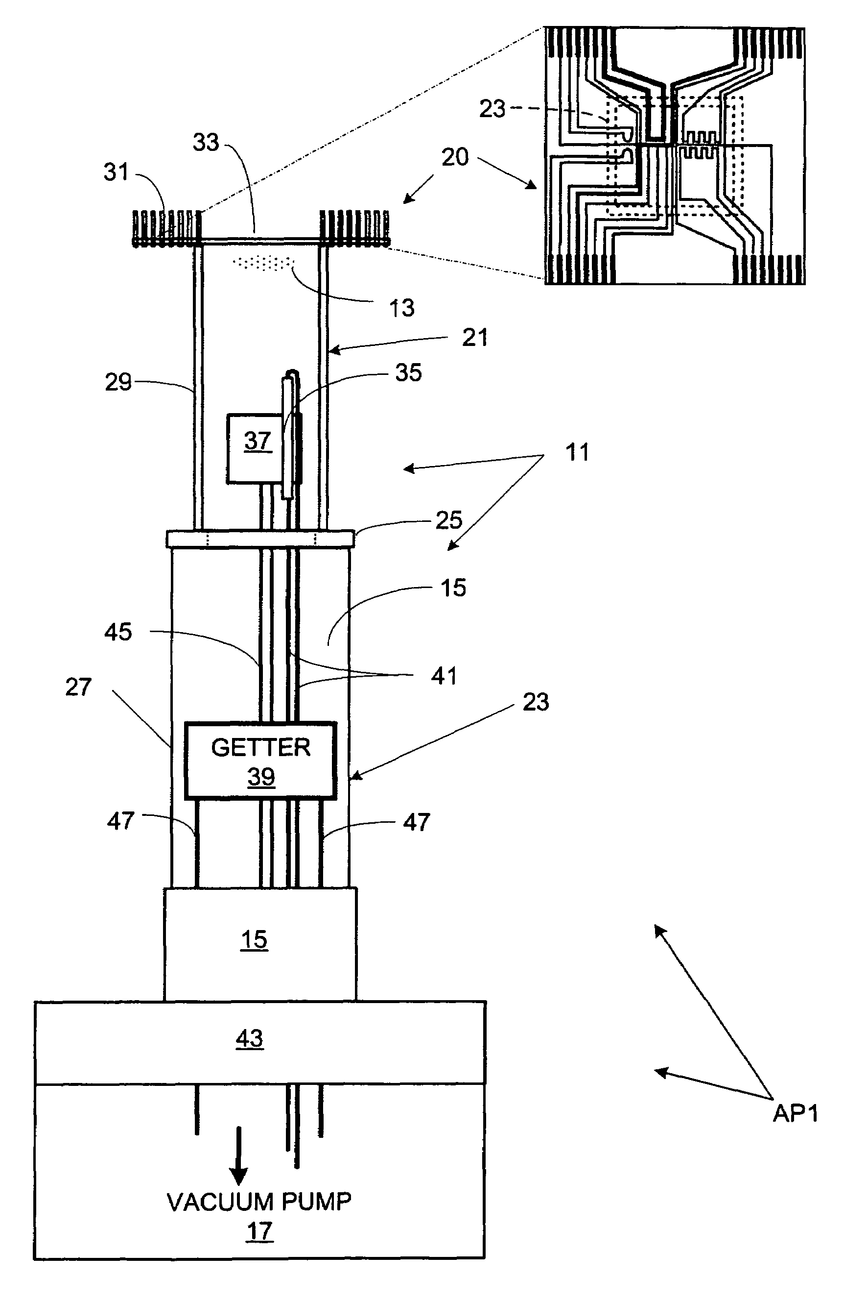
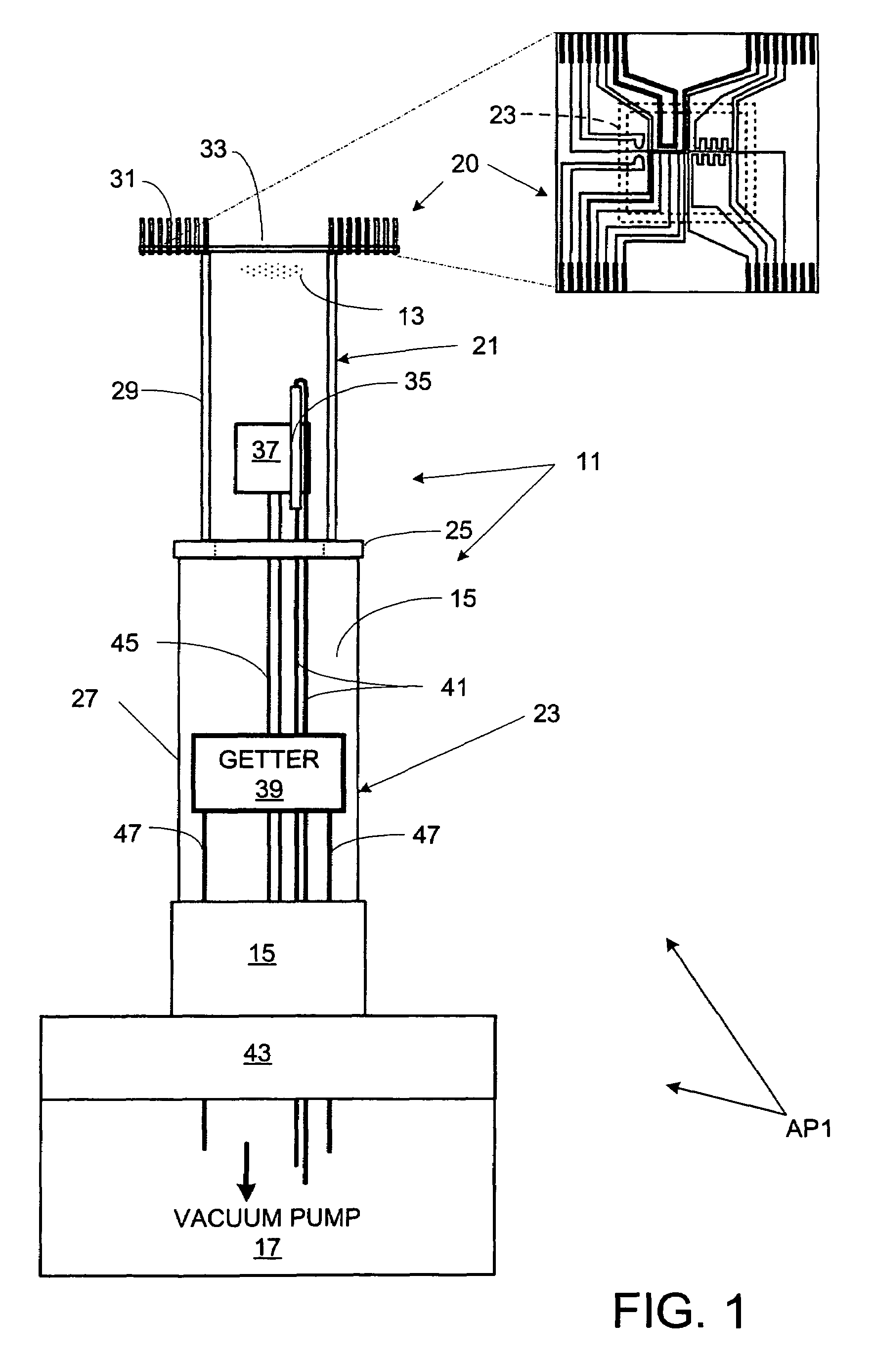
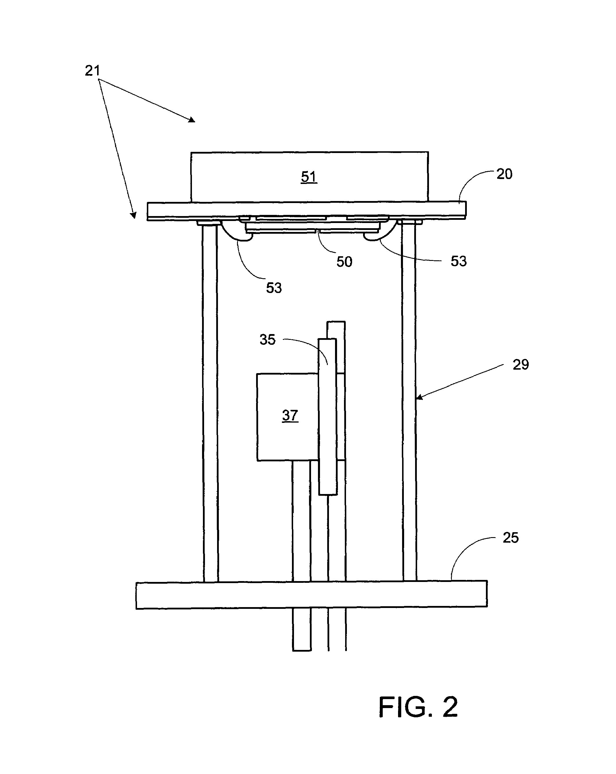
[0024]A cold-atom system API, shown schematically in FIG. 1, includes a novel cold-atom cell 11 (with a Bose-Einstein condensate 13 indicated therein), a glass-to-metal interface 15, and a vacuum pump 17. Cell 11 includes an atom chip 20, a dispenser section 21 and a getter section 23, coupled by a disk 25. Getter section 23 has a cylindrical transparent glass wall 27, while disperser section 21 has four rectangular transparent glass side walls 29 defining a square cross section.

[0025]Atom chip 20 is patterned to define circuits for controlling and sensing atoms in a Bose-Einstein condensate, as shown in the detail of FIG. 1. Atom chip 20 servers as a top wall for dispenser section 21 and cold-atom cell 11, but extends laterally beyond walls 29, indicated in dash in the detail. This allows leads 31 of atom chip 20 to be positioned laterally from dispenser section 21 of atom cell 20, leaving a central area 33 accessible for on-chip active elements. In addition, the lead-free area 33 ...


PUM


Abstract

A compact vacuum chamber gives electric and optical access to a microchip, which is part of the chamber. The main use of the microchip is to confine, cool and manipulate cold atoms (atom chip). The main new feature is that the microchip forms one wall of a vacuum cell. This makes the chamber compact and lightweight, provides large optical access combined with small overall size, eliminates in-vacuum cabling, and makes the back surface of the chip accessible from the outside (e.g., for cooling and / or additional field-producing elements).

Description

[0001]This application claims the benefit from the filing data for U.S. Provisional Patent Application No. 60 / 552,319 filed Mar. 10, 2004. This application is incorporated in its entirety herein by reference.BACKGROUND OF THE INVENTION[0002]The present invention relates to cold-atom chips and, more particularly, to vacuum cells for sensing and manipulating cold atoms. A major objective of the invention is to provide an improved cold-atom vacuum cell.[0003]Cold atoms and ions are on the way from the research lab to technical applications such as 1) atom interferometry, e.g., used for ultra sensitive sensors (M. A. Kasevich. Coherence with Atoms. Science, 298, 1363 (2002)); 2) time and frequency standards; and 3) quantum information processing. All current cold atom and ion applications require an ultrahigh vacuum (UHV) apparatus with optical access. In addition, a multipolar electrical feedthrough is typically required when cold atoms are produced and manipulated with atom chips (J. ...

Claims


Application Information

Patent Timeline
Patent Type & Authority Patents(United States)
IPC IPC(8): H01S1/00H01S3/00H05H3/02H01L29/06H01L31/0328H01L31/0336
CPCG21K1/006G01N21/03
Inventor ANDERSON, DANA Z.REICHEL
Owner COLDQUANTA
Why Eureka
Try Eureka