Closed region defect detection system

a defect detection and closed-area technology, applied in the field of electronic inspection systems, can solve the problems of high cost of comparison-type inspection systems, increased complexity of integrated circuits, and high cost of inspection process

Active Publication Date: 2006-10-24
KLA TENCOR TECH CORP
View PDF8 Cites 37 Cited by
  • Summary
  • Abstract
  • Description
  • Claims
  • Application Information

AI Technical Summary

Benefits of technology

[0013]The present system has the ability to simultaneously detect defects, particularly those associated with contacts on the surface of test and reference specimens, such as photomasks, using transmitted and/or reflected light energy or flux received. In accordance with the present invention there is provided a novel method and apparatus for the inspection of photomasks at a high sensitivity to detect submic

Problems solved by technology

As the complexity of integrated circuits has increased, so has the demand on the inspection process.
These comparison-type inspection systems are quite expensive because they rely on pixel-by-pixel comparison of all the dies and, by necessity, rely on highly accurate methods of alignment between the two dies used at any one time for the comparison.
Apart from their high costs, this method of inspection is also unable to detect particles on light blocking parts of the reticle which have the tendency to subsequently migrate to parts that are transparent and then cause a defect on the wafer.
Unfortunately, the edges of the pattern also cause scattering and for that reason these systems can in certain circumstances be unreliable for the detection of particles smaller than one micrometer.
Even with these newer photomask and wafer inspection techni

Method used


Image

  • Closed region defect detection system
  • Closed region defect detection system
  • Closed region defect detection system

Examples


Embodiment Construction

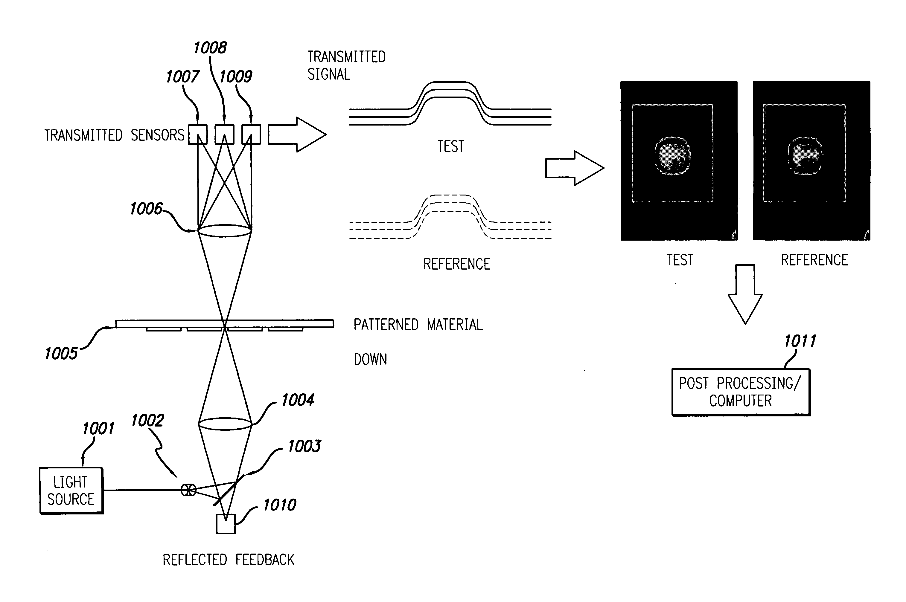
[0035]A general representation of a system employing the current design is presented in FIG. 10. From FIG. 10, a light source 1001 emits light energy or flux toward a set of lenses 1002, which expands the light energy toward a beamsplitter / reflector 1003. The light may be any form of radiation, including but not limited to laser light, sufficient to illuminate the wafer and be detected by the sensors 1007–1009. Light energy is reflected to lens or lensing arrangement 1004, and to the specimen, such as a wafer 1005, where in the case of a wafer the patterned side is downward in the orientation shown. The patterned side is in certain circumstances referred to as the chrome side or metal side, but other materials may be used. The opposite side of the wafer or specimen typically is composed of a transparent or semitransparent material, commonly referred to as glass. In this configuration, light exposure of the specimen will reflect from the patterned material and pass through areas wher...


PUM


Abstract

A method and apparatus for inspecting specimens or patterned transmissive substrates, such as photomasks, for unwanted particles and features, particularly those associated with contacts, including irregularly shaped contacts. A specimen is illuminated by a laser through an optical system comprised of a laser scanning system, individual transmitted and/or reflected light collection optics and detectors collect and generate signals representative of the light transmitted by the substrate. The defect identification of the substrate is performed using those transmitted light signals. Defect identification is performed using an inspection algorithm by comparing image feature representations of a test specimen with a reference specimen, and using a boundary computer and flux comparison device to establish tight boundaries around contacts and compute flux differences between the test and reference specimen contacts. Defect sizes are reported as ratio of flux difference, and entire contacts are highlighted for review.

Description

[0001]This application claims the benefit of U.S. Provisional Patent Application Ser. No. 60 / 375,091, filed Apr. 23, 2002.BACKGROUND OF THE INVENTION[0002]1. Field of the Invention[0003]The present invention relates generally to electro-optical inspection systems, and more particularly to a method or algorithm for automated photomask inspection to detect defects on optical masks, reticles, and the like.[0004]2. Description of the Related Art[0005]Integrated circuits are made by photolithographic processes which use photomasks or reticles and an associated light source to project a circuit image onto a silicon wafer. A high production yield is contingent on having defect free masks, reticles, and wafer surfaces.[0006]Automated mask inspection systems have existed for several years. One of the earliest such systems used a laser that scanned the mask. Subsequent systems used a linear sensor to inspect an image projected by the mask using die-to-die inspection, i.e., inspection of two a...

Claims


Application Information

Patent Timeline
IPC IPC(8): G01N21/00
CPCG01N21/9501G01N21/956
Inventor CHEN, GEORGE Q.YIIN, LIH-HUAHCAO, YU
Owner KLA TENCOR TECH CORP
Why Eureka
Try Eureka