Current sensor and current sensor manufacturing method

a manufacturing method and current sensor technology, applied in the field of current sensor, can solve the problems of low cost, inconvenient miniaturization of current sensor, and sensor not suitable for mass production, and achieve the effect of reducing the width of the current conductor and substantially increasing the detection sensitivity of the magnetic field detection elemen

Inactive Publication Date: 2006-10-31
ASAHI KASEI ELECTRONICS CO LTD +1
View PDF11 Cites 67 Cited by
  • Summary
  • Abstract
  • Description
  • Claims
  • Application Information

AI Technical Summary

Benefits of technology

[0025]As for the sixth aspect of the present invention, the detection sensitivity of the magnetic field detection element is substantially increased by reducing a width of the current conductor where the magnetic field detection element is placed on.
[0042]As for the eleventh aspect of the present invention, on the manufacturing method of the current sensor mentioned in the seventh through tenth aspect, the detection sensitivity of the magnetic field detection element is substantially increased by reducing a width of the current conductor where the magnetic field detection element is placed on.

Problems solved by technology

However, the current sensor having the configuration of FIG. 1 is not suitable for miniaturization because the sensor requires a magnetic core 4 surrounding a current conductor 2 fed with current.
Further, since the magnetic core 4 and a Hall element 6 need to be separately manufactured and then assembled into one, the sensor has not been suitable for mass production and the cost is not low.
For this reason, it is difficult to detect current with high sensitivity.
However, the invention is not practical and lacks mass productivity, considering complexity of a method of fixing the magnetic field sensor chip on the current conductor and a wire bonding method between a sensor chip terminal and a lead frame.
Thus, it is difficult to detect accurately a flux generated by the current to be measured.
Thus, it is difficult to form the lead frame and a current conductor in the process of packaging.
(4) Proper shielding has not been sufficiently performed in the case where a flux generated by disturbance or an external interference magnetic field exists around the magnetic field sensor.
In an actual one-chip current sensor, it has not been achieved efficiently yet.

Method used


Image

  • Current sensor and current sensor manufacturing method
  • Current sensor and current sensor manufacturing method
  • Current sensor and current sensor manufacturing method

Examples


embodiment 1

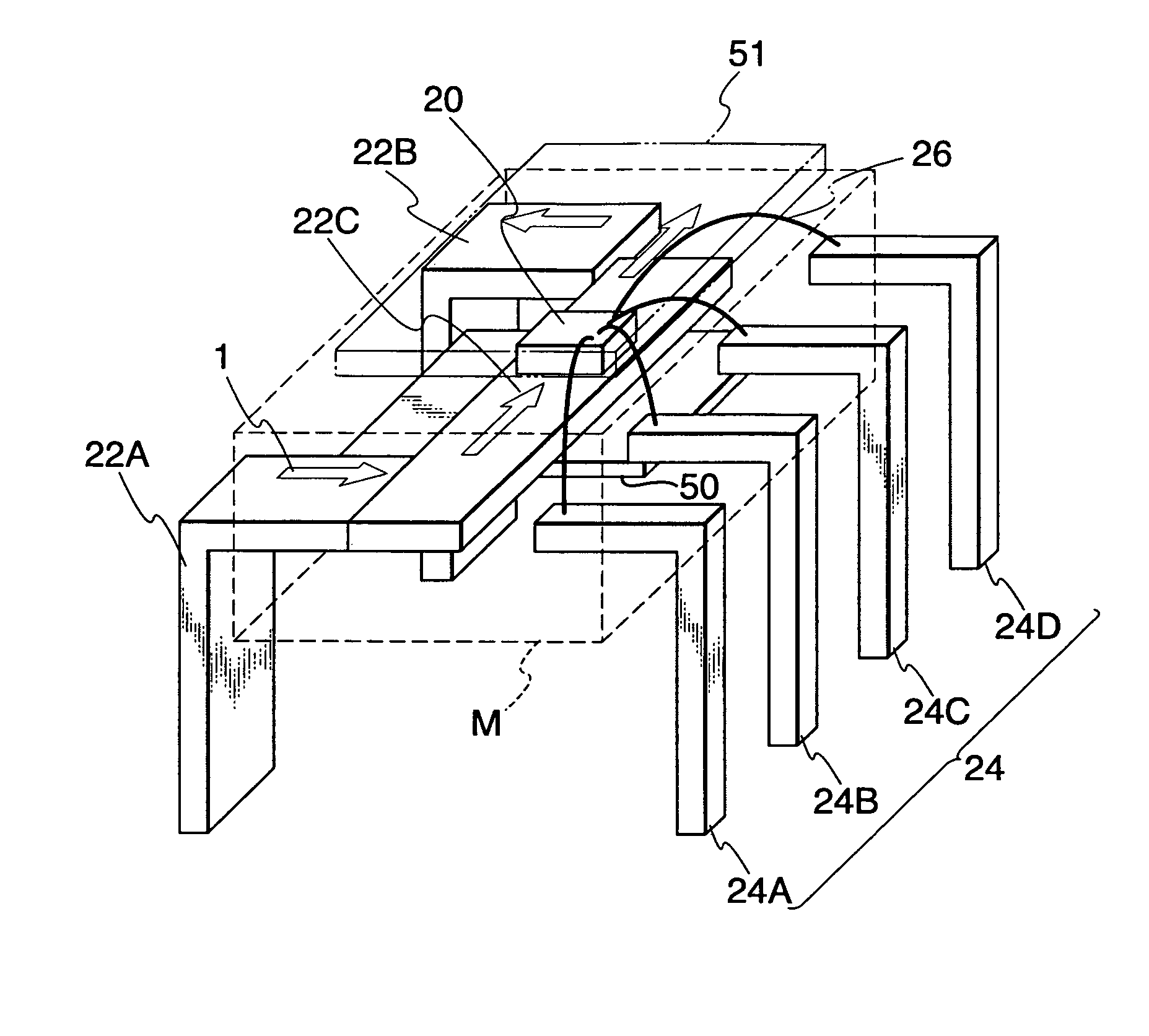
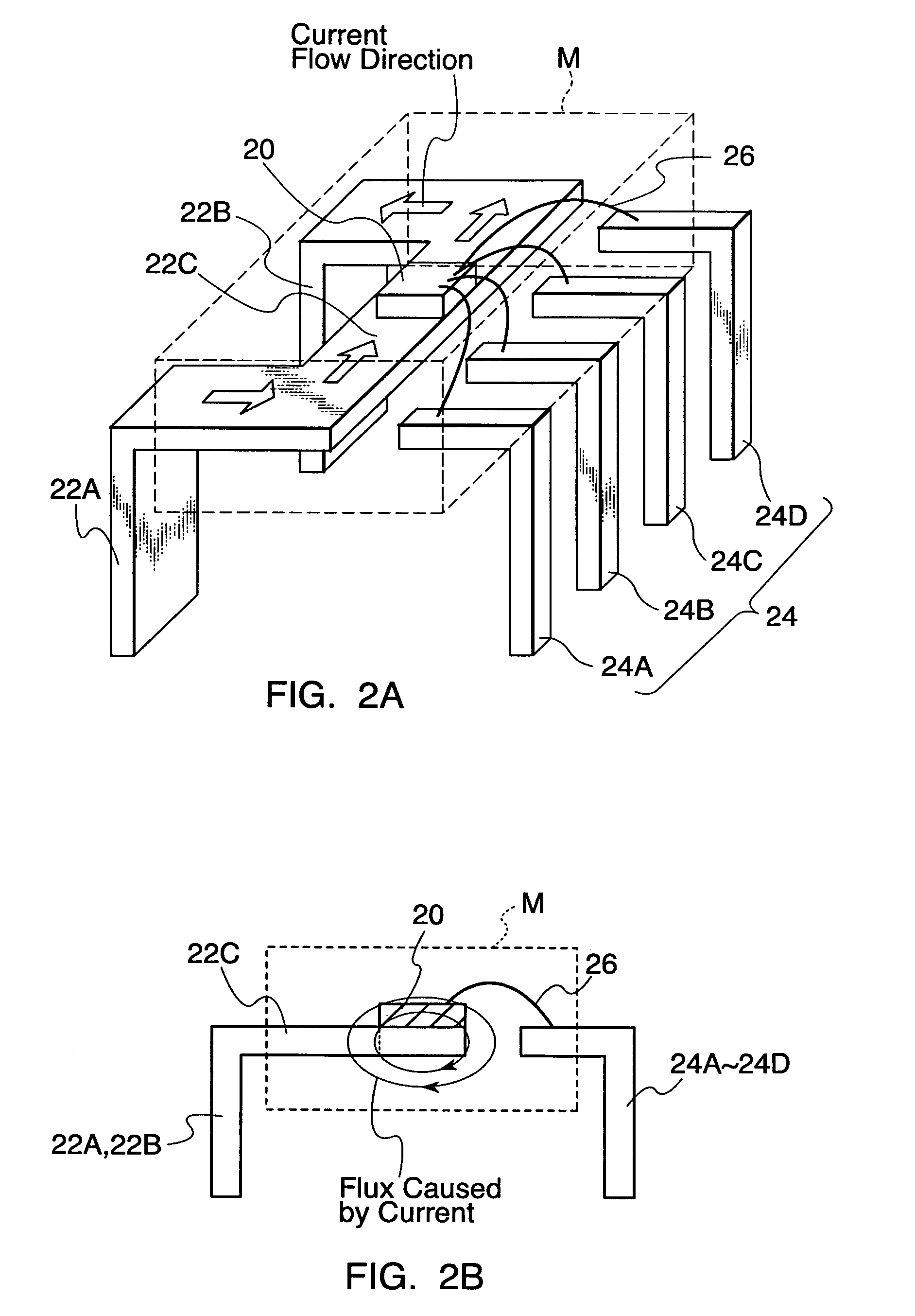
[0074]FIG. 2A is a perspective view showing schematically the entire configuration of a current sensor employing the present invention. FIG. 2B is a view showing schematically the configuration of the current sensor shown in FIG. 2A. In these views, reference numeral 20 denotes a magnetic field sensor chip including a magnetic field detection element like a Hall element and so on, reference numerals 22A to 22C denote current conductors for applying a current to be measured, and reference numerals 24A to 24D denote lead frame terminals. Each of the lead frame terminals 24A to 24D and the current conductor 22A to 22C are formed from a single thin plate-like metal as will be discussed later (FIG. 4A and FIG. 4B). Reference numeral 26 denotes a bonding wire for connecting the lead frame terminals 24A to 24D and the magnetic field sensor chip 20. Further, reference character M denotes a part to be molded in plastics.

[0075]FIGS. 3A, 3B, and 3C are, respectively, a perspective view, a sect...

embodiment example

[0080]The following will discuss an embodiment example corresponding to FIG. 2A.

[0081]A copper plate with a thickness of 0.4 mm was used as a thin plate-like metal (FIG. 4A) to form the current conductor 22A to 22C and the lead frame terminals 24A to 24D as one. As described above, FIG. 4A shows that a plurality of chips are connected. Manufacturing in large quantity was readily performed by using completely the same process used for lead frames of a typical integrated circuit. Then the above lead frames were used to form a current sensor molded in plastics used for an integrated circuit. This is shown in FIG. 4B.

[0082]The width of the center part 22C of the current conductor placing the magnetic field sensor chip 20 thereon was about 2 mm, and the outside of the molded plastics was about 5.5 mm in width, and a maximum current of 25A could be applied continuously. The Hall ASIC shown in FIGS. 3B and 3C was applied on the magnetic field sensor chip 20. The Hall ASIC was fixed on an i...

embodiment 2

[0084]FIGS. 5A and 5B are schematical perspective views showing the entire configuration of a current sensor corresponding to another embodiment. In these views, in addition to the configuration of FIG. 2, a soft thin plate-like magnetic material 50 is bonded beneath a current conductor 22C (that is, bonded on the opposite side from a magnetic field sensor chip 20).

[0085]FIGS. 6A, 6B, and 6C are explanatory drawings showing the function of the soft, thin plate-like magnetic material 50 shown in FIGS. 5A and 5B.

[0086]As shown in FIGS. 5A, 5B, 6A, 6B, and 6C, the soft, thin plate-like magnetic material 50 with high magnetic permeability, high saturation flux density, and low coercive force is bonded on the backside of an island part 22C of the current conductor, so that the soft, thin plate-like magnetic material 50 absorbs an external flux entering from the outside of the current sensor, and that it passes through the plate 50. Thus, it is possible to reduce influence of the external...


PUM


Abstract

A low-cost, current sensor suitable for mass production and a manufacturing method thereof are provided. The current sensor is small with high sensitivity and can be packaged in a standard assembly line which is normally used when an integrated circuit is manufactured. Further, it is possible to obtain a sufficient shielding effect against a disturbance flux without degrading the detecting sensitivity of a flux. A first magnetic material 50 is bonded to the lower part of a current conductor 22C. The first magnetic material 50 has the function of converging and amplifying a flux 3 generated by the current to be measured. A second magnetic material 51 is bonded above a magnetic sensor chip 20. The second magnetic material 51 has a shielding function against a disturbance flux entering from the outside.

Description

CROSS REFERENCE TO RELATED APPLICATIONS[0001]This Application is a 371 of PCT / JP02 / 11473, filed Nov. 01, 2002.[0002]The present application is related to and claims priority of the following co-pending applications, namely, PCT application number PCT / JP02 / 11473 of Sentron AG and ASAHI KASEI EMD CORPORATION entitled “Current Sensor and Current Sensor Manufacturing Method”, filed on Nov. 1, 2002; and JP Application No. 2001-336682, filed Nov. 1, 2001. The above-identified applications are incorporated herein by reference in their entirety.BACKGROUND OF THE INVENTION[0003]1. Field of the Invention[0004]The present invention relates to a current sensor and a method of manufacturing the current sensor.[0005]To be specific, the present invention relates to a current sensor of magnetoelectric conversion type, which measures the intensity of a current by detecting a flux generated by the current to be measured with a magnetic field detection element, and a manufacturing method thereof.[0006...

Claims


Application Information

Patent Timeline
Patent Type & Authority Patents(United States)
IPC IPC(8): G01R15/20
CPCG01R15/20G01R15/202G01R15/207H01L2224/48091H01L2224/48247H01L2924/00014G01R31/00
Inventor SHIBAHARA, KOJIPOPOVIC, RADIVOJEYAMAGATA, YORACZ, ROBERT
Owner ASAHI KASEI ELECTRONICS CO LTD
Why Eureka
Try Eureka