Efficient implementation of a bypassable flip-flop with a clock enable

a flip-flop and clock enable technology, applied in the field of flip-flops, can solve the problems of unfavorable increase of signal propagation delay in the flip-flop, and achieve the effects of reducing the number of pass gates, reducing the capacitive load, and reducing the clock-to-out delay of the flip-flop

Active Publication Date: 2006-10-31
XILINX INC
View PDF3 Cites 34 Cited by
  • Summary
  • Abstract
  • Description
  • Claims
  • Application Information

AI Technical Summary

Benefits of technology

[0005]A flip-flop circuit is disclosed that implements the bypass and clock enable / disable features using circuitry that minimizes silicon area and reduces signal propagation delays. In accordance with the present invention, a flip-flop circuit includes a flip-flop, a first pass gate, a second pass gate, and a third pass gate. The first pass gate has an input to receive an input signal, an output coupled to a data input of the flip-flop, and a control terminal to receive a first control signal. The second pass gate has a first data terminal to the data input of the flip-flop, a second data terminal output coupled to an output of the flip-flop circuit, and a control terminal to receive a second control signal. The third pass gate has an input coupled to a data output of the flip-flop, an output coupled to the output of the flip-flop circuit, and a control terminal to receive a third control signal.
[0007]In accordance with some embodiments of the present invention, the second pass gate is configured to operate as a bi-directional pass gate that can not only propagate the input signal directly to the flip-flop circuit's output without passing through the flip-flop (e.g., when the bypass mode is selected), but also propagate the flip-flop's output as a feedback signal to the data input of the flip-flop (e.g., when the clock disable mode is selected). In this manner, flip-flop circuits of the present invention may use the same pass gate to implement the bypass and clock enable / disable features, thereby reducing the number of pass gates required to implement the bypass and clock enable / disable features, for example, as compared to prior flip-flop circuits. Further, by reducing the number of pass gates coupled to the flip-flop's output, embodiments of the present invention may also reduce the capacitive load on the flip-flop's output, which in turn advantageously reduces the flip-flop's clock-to-out delay, for example, as compared to prior flip-flop circuits.

Problems solved by technology

Although effective, prior techniques for implementing the clock enable / disable and bypass features of a flip-flop circuit not only consume valuable silicon area but also increase the capacitive loading on the flip-flop's input and output terminals, thereby undesirably increasing signal propagation delays in the flip-flop.

Method used


Image

  • Efficient implementation of a bypassable flip-flop with a clock enable
  • Efficient implementation of a bypassable flip-flop with a clock enable
  • Efficient implementation of a bypassable flip-flop with a clock enable

Examples


Embodiment Construction

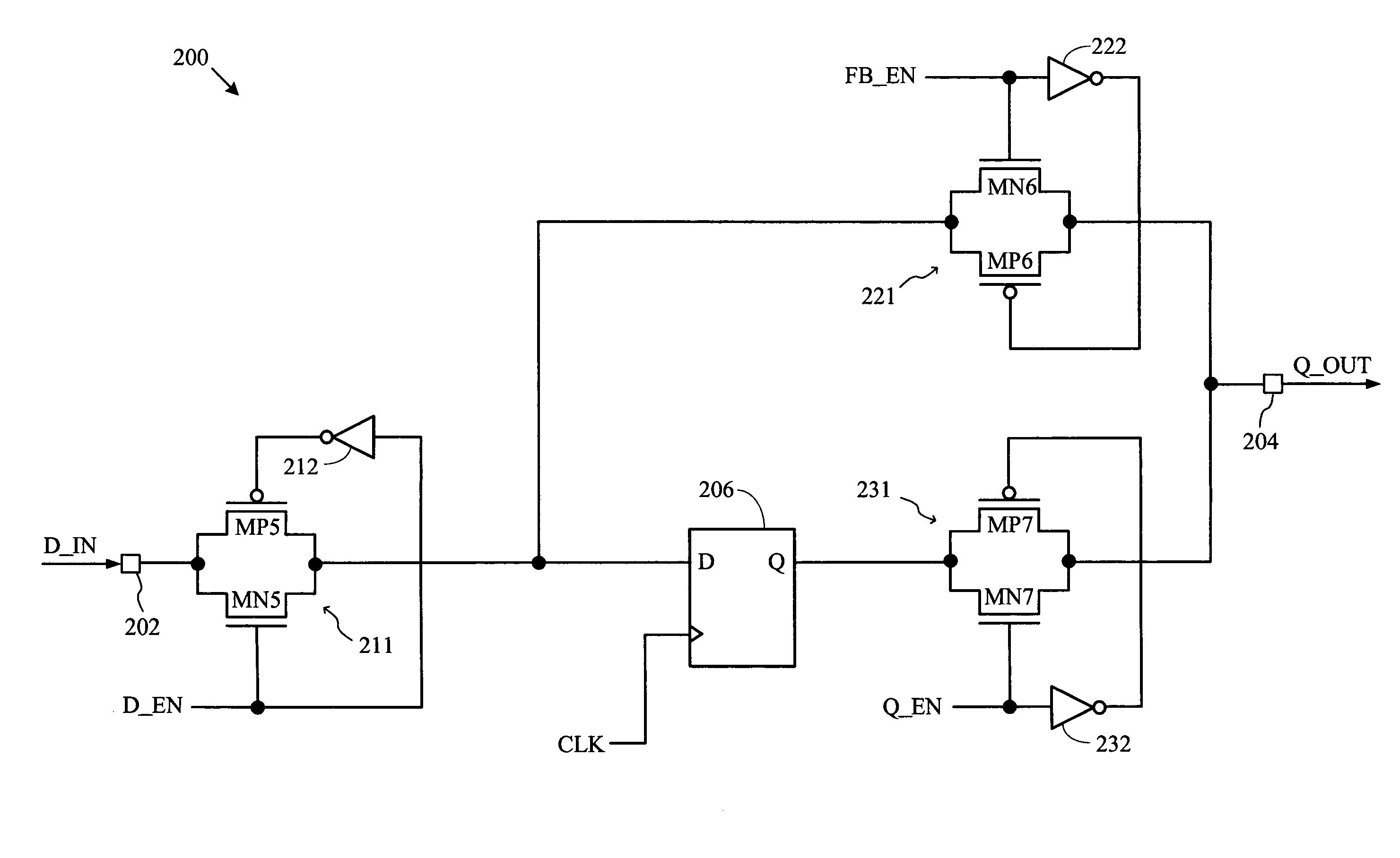
[0018]Embodiments of the present invention are applicable to a variety of integrated circuits and systems, and are particularly useful for devices requiring flip-flop circuits that include bypass and clock enable / disable features. In the following description, for purposes of explanation, specific nomenclature is set forth to provide a thorough understanding of the present invention. In other instances, well-known circuits and devices are shown in block diagram form to avoid obscuring the present invention unnecessarily. Further, the logic levels assigned to various signals in the description below are arbitrary, and thus may be modified (e.g., reversed polarity) as desired. Accordingly, the present invention is not to be construed as limited to specific examples described herein but rather includes within its scope all embodiments defined by the appended claims.

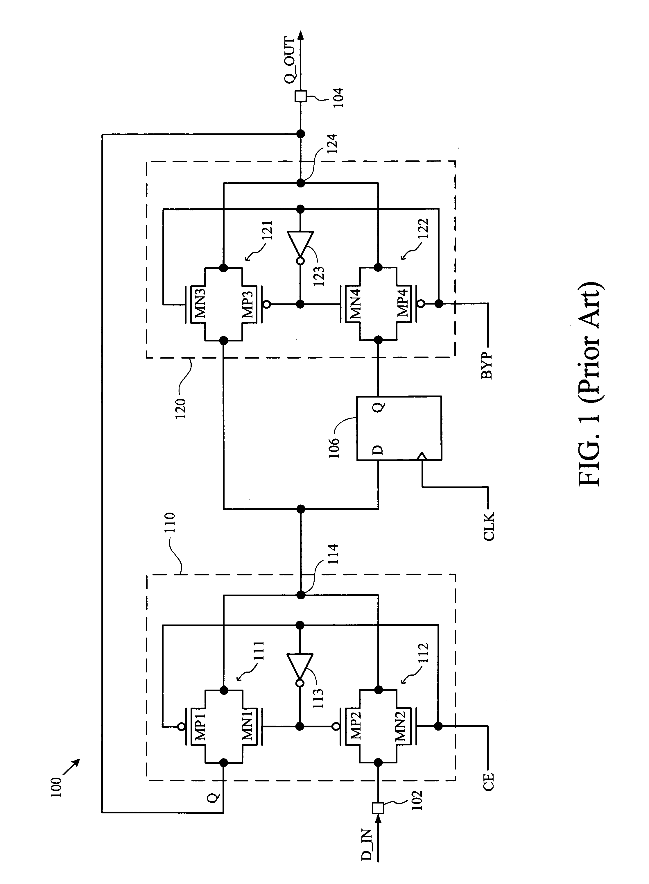
[0019]The present invention overcomes the aforementioned disadvantages of previously known flip-flop circuits by using com...


PUM


Abstract

A flip-flop circuit includes a flip-flop, a first pass gate, a second pass gate, and a third pass gate. The first pass gate has an input to receive an input signal, an output coupled to the flip-flop's data input, and a control terminal to receive a first control signal. The second pass gate has an input coupled to the flip-flop's data input, an output coupled to the circuit's output, and a control terminal to receive a second control signal. The third pass gate has an input coupled to the flip-flop's data output, an output coupled to the circuit's output, and a control terminal to receive a third control signal. The first, second, and third control signals may be generated in response to various logical combinations of a bypass signal and a clock enable signal.

Description

FIELD OF INVENTION[0001]This invention relates to a flip-flop capable of implementing a bypass feature and a clock enable / disable feature.DESCRIPTION OF RELATED ART[0002]A flip-flop is a well-known circuit element that is commonly used to hold the logic state of a signal in a variety of clocked integrated circuit (IC) systems such as, for example, programmable logic devices (PLDs). Many flip-flops include a bypass feature that is controlled by a bypass signal. When the bypass signal is asserted, the signal bypasses the flip-flop, thereby allowing the signal to be routed asynchronously to other circuitry coupled to the flip-flop. When the bypass signal is de-asserted, logic state transitions of the signal are latched in the flip-flop in response to triggering edges of a clock signal for subsequent output from the flip-flop. Further, many flip-flops also include a clock enable / disable feature that is controlled by a clock enable signal. When the clock enable signal is asserted, logic ...

Claims


Application Information

Patent Timeline
Patent Type & Authority Patents(United States)
IPC IPC(8): H03K3/12H03K3/289
CPCH03K3/012H03K3/037
Inventor VADI, VASISHT MANTRA
Owner XILINX INC
Why Eureka
Try Eureka