Excimer laser inspection system

a laser inspection and excitation technology, applied in the field of optical imaging, can solve the problems of low power density, low efficiency, and low power density of current inspection systems, and achieve the effects of improving the efficiency of inspection systems, reducing the cost of inspection, and improving the efficiency of inspection

Inactive Publication Date: 2006-11-14
KLA TENCOR TECH CORP
View PDF78 Cites 71 Cited by
  • Summary
  • Abstract
  • Description
  • Claims
  • Application Information

AI Technical Summary

Problems solved by technology

The inspection systems currently available are highly complex, requiring a sophisticated combination of light source, illumination, imaging, positioning, automatic focusing, image sensor, data acquisition, and data analysis subsystems.
However, relatively constant and non-pulsed energy sources suffer from particular drawbacks.
Few non-pulsed sources are available with the re

Method used


Image

  • Excimer laser inspection system
  • Excimer laser inspection system
  • Excimer laser inspection system

Examples


Embodiment Construction

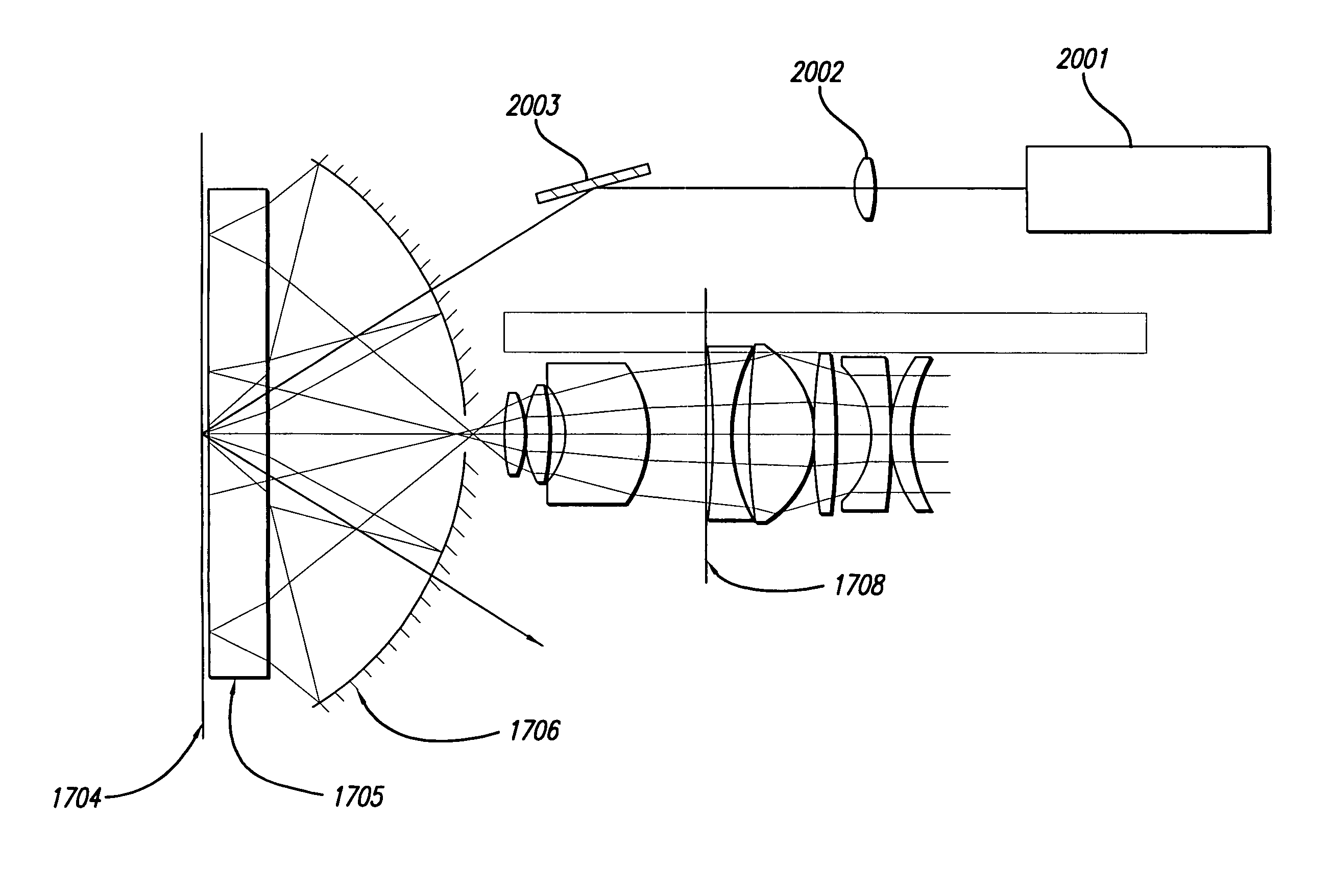
[0069]The inspection system disclosed herein employs an excimer illumination subsystem having advantages over non-pulsed designs. FIG. 1 illustrates a typical inspection subsystem having an illumination subsystem 101, positioning stage 102, autofocus subsystem 103, imaging subsystem 104, sensor subsystem 105, data acquisition subsystem 106, and data analysis subsystem 107. The light path travels from the illumination subsystem 101 to the positioning stage 102, the imaging subsystem 104, and the sensor subsystem 105. Data passes between the autofocus subsystem 103 and the positioning stage 102, between the sensor and the data acquisition subsystem, and between the data acquisition subsystem and the illumination subsystem and the data analysis subsystem, and between the data analysis subsystem and the positioning stage.

[0070]Inspection Modes

[0071]Many different modes exist for inspecting partially fabricated integrated circuits and photomasks. Potential inspection modes include bright...


PUM


Abstract

A system and method for inspecting a specimen, such as a semiconductor wafer, including illuminating at least a portion of the specimen using an excimer source using at least one relatively intense wavelength from the source, detecting radiation received from the illuminated portion of the specimen, analyzing the detected radiation for potential defects present in the specimen portion.

Description

[0001]This application is a continuation in part of U.S. patent application Ser. No. 09 / 796,117, filed Feb. 28, 2001, now U.S. Pat. No. 6,842,298 entitled “Broad Band DUV / VUV Long Working Distance Catadioptric Imaging System,” inventors Shafer et. al., which claims the benefit of U.S. Provisional Patent Application 60 / 231,761, filed Sep. 12, 2000.BACKGROUND OF THE INVENTION[0002]1. Field of the Invention[0003]The present invention relates generally to the field of optical imaging and more particularly to optical systems for microscopic imaging, inspection and / or lithography applications.[0004]2. Description of the Related Art[0005]Many optical systems and electronic systems are available to inspect surface features of a specimen for defects, including specimens such as a semiconductor photomask or partially fabricated integrated circuit. Defects on such specimens may take the form of particles randomly localized on the specimen surface, scratches, process variations, repeating patte...

Claims


Application Information

Patent Timeline
IPC IPC(8): G01N21/00G01N21/95G02B17/08G02B21/04G03F7/20
CPCG01N21/8806G01N21/9501G01N21/95607G02B17/0808G02B17/0856G02B17/0892G02B21/04G03F7/70225G01N2021/479G01N2021/8825G01N2021/95676G01N2201/06113
Inventor TSAI, BIN-MING BENJAMINCHUANG, YUNG-HOARMSTRONG, J. JOSEPHBROWN, DAVID LEE
Owner KLA TENCOR TECH CORP
Why Eureka
Try Eureka