Laser scanning device

a laser scanning and laser technology, applied in the field of laser scanning devices, can solve the problems of increasing the consumption of toner, deteriorating the sharpness of the edge insufficient density thickness of the image pattern, so as to prevent the deterioration of the image quality due to the rising delay

Inactive Publication Date: 2006-11-14
ASAHI KOGAKU KOGYO KK
View PDF1 Cites 8 Cited by
  • Summary
  • Abstract
  • Description
  • Claims
  • Application Information

AI Technical Summary

Benefits of technology

[0010]The present, invention is advantageous in that the deterioration of the image quality due to the rising delay is prevented.

Problems solved by technology

When such a phenomenon occurs, since the entire light amount is lower than necessary, toner applied to the latent image is reduced, and thus, the image pattern exhibits insufficient density thickness.
Further, the sharpness of the edge of the image pattern may be deteriorated.
In this case, the density thickness of the image pattern may be too thick, and the consumption of the toner increases.
However, such a control is very complicated to apply to the laser scanning device, and may not meet the requirement for the high-speed and high-quality imaging.

Method used


Image

  • Laser scanning device
  • Laser scanning device
  • Laser scanning device

Examples


first embodiment

[0035

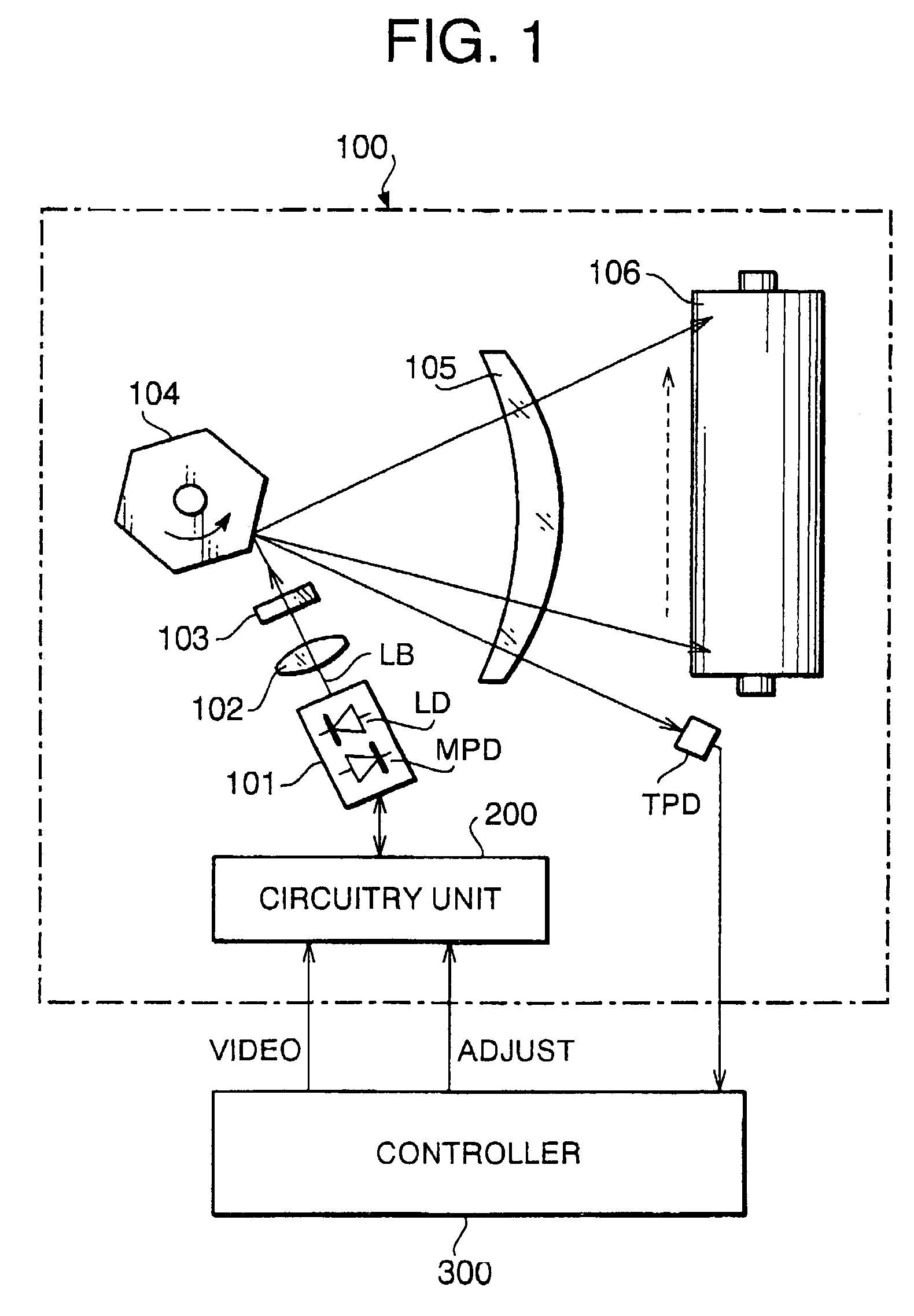
[0036]FIG. 1 schematically shows a configuration of a laser scanning device to which the present invention is applicable.

[0037]The laser scanning device includes a scanning unit 100, a circuitry unit 200 and a controller 300. The scanning unit 100 includes a light source 101 provided with a laser diode LD, a collimating lens 102 which collimates the laser beam emitted by the laser diode LD, and a beam shaping lens 103 including a cylindrical lens and the like for shaping a cross-sectional shape of the beam, a polygonal mirror 104 which deflects the laser beam to scan in a predetermined angular range, an fθ optical system 105 which functions to move the scanned beam on a surface to be scanned at a predetermined constant speed, and a photoconductive drum 106 having a photosensitive surface which is to be scanned by the scanning beam.

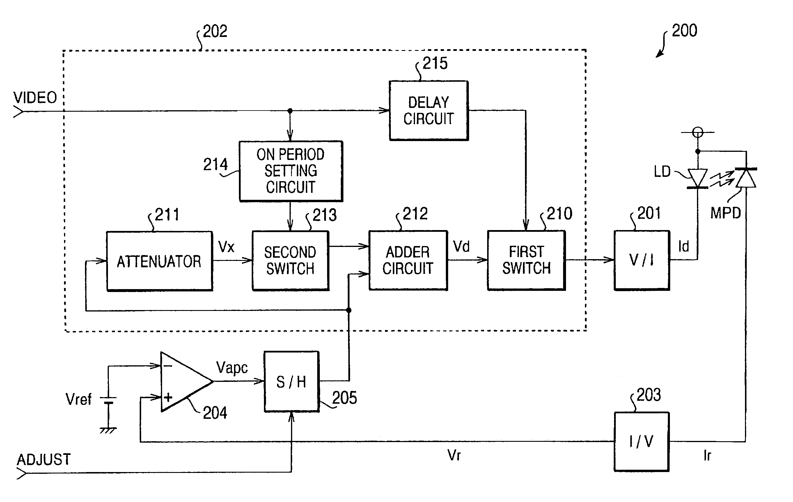
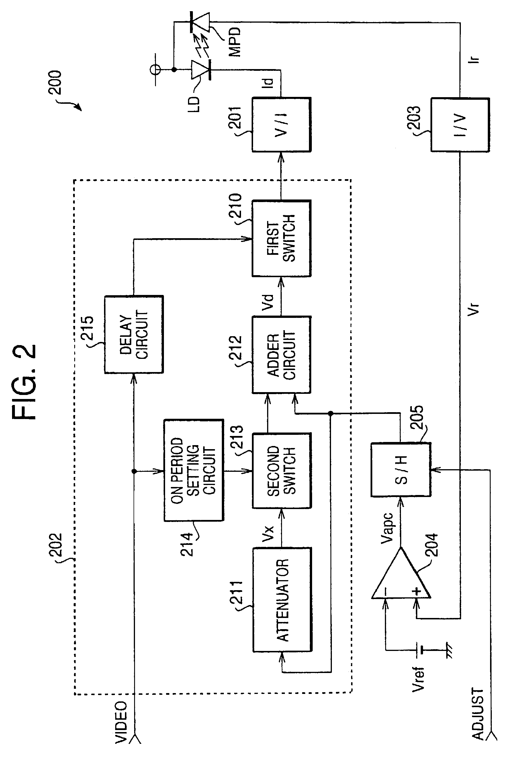
[0038]A monitoring photo diode MPD is implemented in the light source 101 integrally with the laser diode LD. The monitoring photo diode MPD receives...

second embodiment

[0051

[0052]FIG. 5 is a block diagram showing an electrical configuration of a circuitry unit 200A according to a second embodiment. It should be noted that components similar to those in the first embodiment shown in FIG. 2 have the same reference numbers as in FIG. 2, and description thereof will not be repeated herein.

[0053]The circuitry unit 200A has a rising control circuit 202A, which includes the adder circuit 212 for adding an APC voltage Vapc sampled and held by the sample-hold circuit 205 and the compensating voltage Vx, the second switch circuit 213 for switching the compensating voltage Vx applied to the adder circuit 212, the ON period setting circuit 214 for turning ON the second switch circuit 213 for a certain period of time in accordance with the video signal VIDEO, and the delay circuit 215 for delaying the ON period of the first switch circuit 210 in accordance with the video signal VIDEO, as in the first embodiment.

[0054]A circuit for attenuating the APC voltage V...

third embodiment

[0059

[0060]FIG. 6 is a block diagram showing a circuitry unit 200B of the electrical configuration of the laser scanning device according to a third embodiment. It should be noted that components similar to those in the second embodiment shown in FIG. 5 are indicated by the same reference numbers as in FIG. 5, and description thereof will not be repeated herein. It should be noted that a first adder circuit 212 of the third embodiment is equivalent to the adder circuit 212 in the first and second embodiments.

[0061]In the circuitry unit 200B, a rising control circuit 202B is configured such that a bias reference voltage circuit 218 and a subtraction circuit 219 are provided in addition to the configuration of the rising control circuit 202A of the second embodiment. The bias reference voltage circuit 218 controls a bias reference voltage Vb of the laser diode LD in accordance with the temperature detected by the temperature detection circuit 217. The subtraction circuit 219 subtracts...


PUM


Abstract

A laser scanning apparatus is provided with a laser diode that is driven to emit a laser beam, a scanning optical system that scans the laser beam emitted by the laser diode on a surface to be scanned, and a controller that drives the laser diode by supplying electrical current to the laser diode. The controller supplies an extra electrical current to the laser diode only at an initial stage of driving of the laser diode so as to cancel an effect of a rising delay of its output intensity.

Description

BACKGROUND OF THE INVENTION[0001]The present invention relates to a laser scanning device that emits a scanning laser beam which is modulated in accordance with video signal or the like.[0002]A laser scanning device has been widely employed in imaging apparatuses. Typically, the laser scanning device is configured such that a laser beam emitted by a laser diode is deflected using a polygonal mirror to scan a predetermined angular range. While the laser beam is deflected, emission of the beam of the laser diode is ON / OFF modulated in accordance with a video signal or the like. The scanning beam is incident on a surface such as a photosensitive surface to be scanned, which surface is moved in a direction perpendicular to the scanning direction, thereby a two-dimensional latent image being formed on the surface.[0003]In such a laser scanning device, in order to compensate for an individual difference of light emission characteristics so that density thickness of the formed image is sta...

Claims


Application Information

Patent Timeline
Patent Type & Authority Patents(United States)
IPC IPC(8): H01S3/13B41J2/44G02B26/10G06K7/10H01S5/042H04N1/036H04N1/113
CPCG06K7/10584G06K7/10851H01S5/042
Inventor SUDA, TADAAKI
Owner ASAHI KOGAKU KOGYO KK
Why Eureka
Try Eureka