Post-placement timing optimization of IC layout

a timing optimization and placement technology, applied in the direction of software simulation/interpretation/emulation, instruments, program control, etc., can solve the problems of difficult to determine the timing constraint of a signal path, high iterative and time-consuming placement and routing process, and more difficult for the algorithm to meet the constraints of other nets

Inactive Publication Date: 2006-11-14
CADENCE DESIGN SYST INC
View PDF5 Cites 16 Cited by
  • Summary
  • Abstract
  • Description
  • Claims
  • Application Information

AI Technical Summary

Problems solved by technology

When timing analysis shows that a layout fails to satisfy timing constraints on some signal paths, the designer may have to modify the layout to reduce path delays in those signal paths.
The placement and routing process can therefore be highly iterative and time-consuming, particularly when many signal paths are tightly constrained.
Although its placement objectives help signal paths meet their timing constraints, such a placement tool does not directly consider timing constraints when placing cells.
But designers often find it difficult to determine how to allocate a signal path's timing constraint among the nets forming a signal path and to select an appropriate weight for each net.
Allocating too large a portion of a time constraint to a net causes a placement algorithm to try to place cells connected to that net closer together than necessary and makes it more difficult for the algorithm to meet constraints on other nets.

Method used


Image

  • Post-placement timing optimization of IC layout
  • Post-placement timing optimization of IC layout
  • Post-placement timing optimization of IC layout

Examples


Embodiment Construction

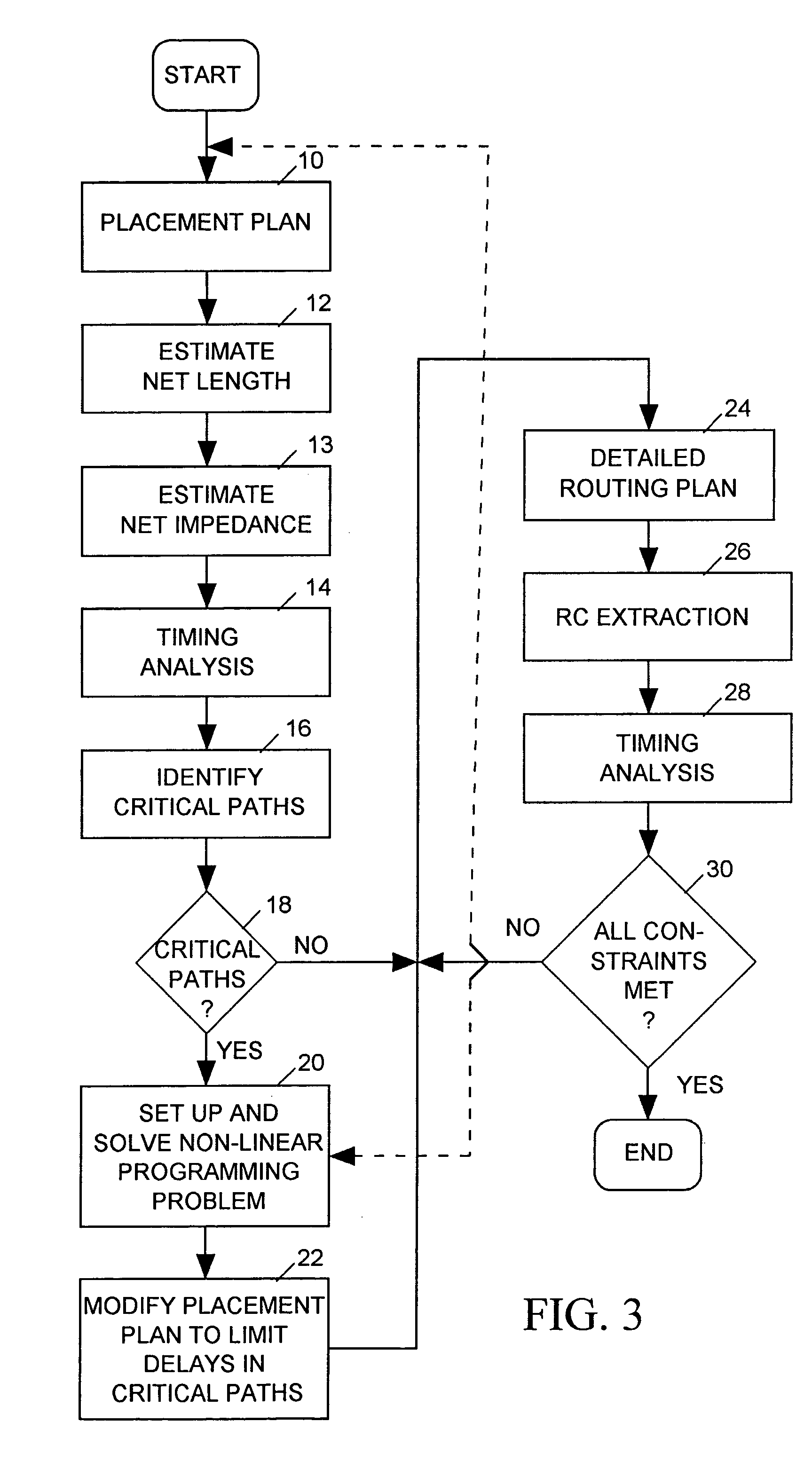
[0032]The present invention relates to a method for optimizing an integrated circuit (IC) placement plan to improve the likelihood that a routing plan based on the placement plan will satisfy signal path timing constraints and to software stored on computer-readable media for enabling a conventional computer to implement that method. Suitable computer-readable media for storing the software include, but are not limited to, compact disks, floppy disks, hard disks, and random access or read only memory. While the specification describes at least one exemplary embodiment of the invention considered a best mode of practicing the invention, the invention is not limited to the particular example(s) described below or to the manner in which they operate.

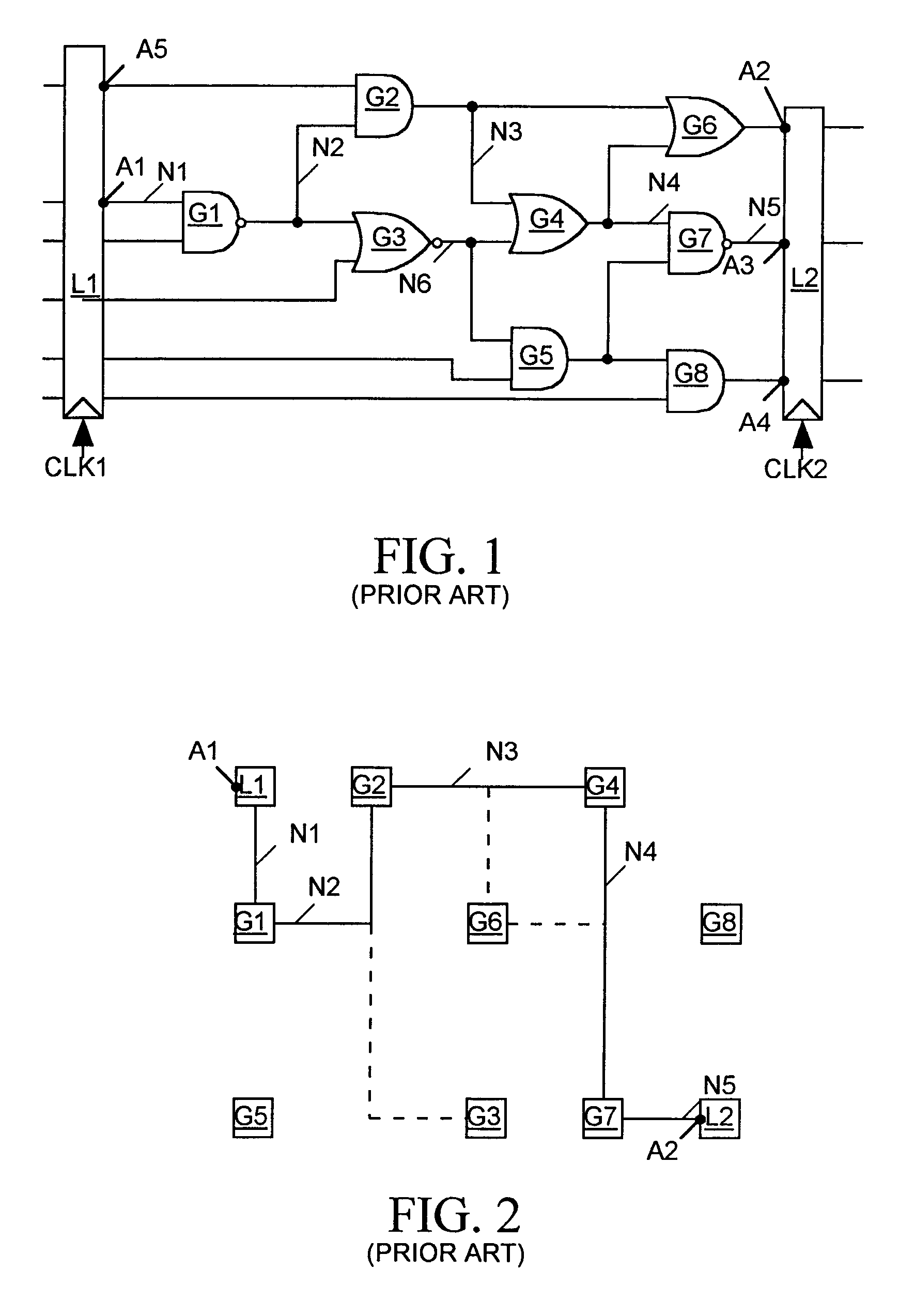
[0033]An IC designer typically produces a high-level language, register transfer level (RTL) netlist describing a digital IC mainly in terms of the logic the IC is to implement. The designer then uses computer-aided synthesis tools to conve...


PUM


Abstract

When an IC layout is to include time-constrained signal paths, a placement plan defining positions of cells forming the IC is analyzed to estimate lengths of nets needed to interconnect the cells based on the positions of cells included in those signal paths. A capacitance and resistance of each net is then estimated based on its estimated length. The delay through each time-constrained signal path is then estimated based on the estimated capacitance and resistance of each net to be included in the time-constrained signal path and on the terminal impedances, switching speeds and driving strengths of the cells included in the signal path. The estimated path delay for each signal path is then compared to its timing constraint to determine whether that signal path is a “critical signal path” likely to fail to meet its timing constraint following development of a detailed routing plan. A non-linear programming technique is then employed to determine how, with minimal disturbance to the placement plan, to reposition cells forming the critical paths so that when the nets are routed between the cells, all critical paths will be more likely to satisfy their timing constraints.

Description

BACKGROUND OF THE INVENTION[0001]1. Field of the Invention[0002]The invention relates in general to methods for generating integrated circuit (IC) placement and routing plans, and in particular to a computer-aided method for optimizing a placement plan to improve the likelihood that a routing plan based on the placement plan will satisfy all timing constraints.[0003]2. Description of Related Art[0004]An IC designer typically generates a hardware description language (HDL) netlist describing an IC in terms of the logical relations between the various IC input, output and internal signals to be conveyed by conductive networks (“nets”) to be formed within the IC. After creating the HDL netlist, the designer uses synthesis tools to convert the HDL netlist into a gate level netlist describing the IC as being formed by a set of instances of logic gates and other types of IC components for implementing the logic described by the HDL netlist. The gate level netlist indirectly describes each...

Claims


Application Information

Patent Timeline
Patent Type & Authority Patents(United States)
IPC IPC(8): G06F17/50G06F9/45G06F9/455
CPCG06F17/5072G06F30/392
Inventor HARN, YWH-PYNG
Owner CADENCE DESIGN SYST INC
Why Eureka
Try Eureka