

Probe station thermal chuck with shielding for capacitive current
a capacitive current and thermal chuck technology, applied in the field of probe stations, can solve the problems of low electrical noise, common noise source, and high noise level
- Summary
- Abstract
- Description
- Claims
- Application Information
AI Technical Summary
Problems solved by technology
Method used
Image

Examples
Embodiment Construction
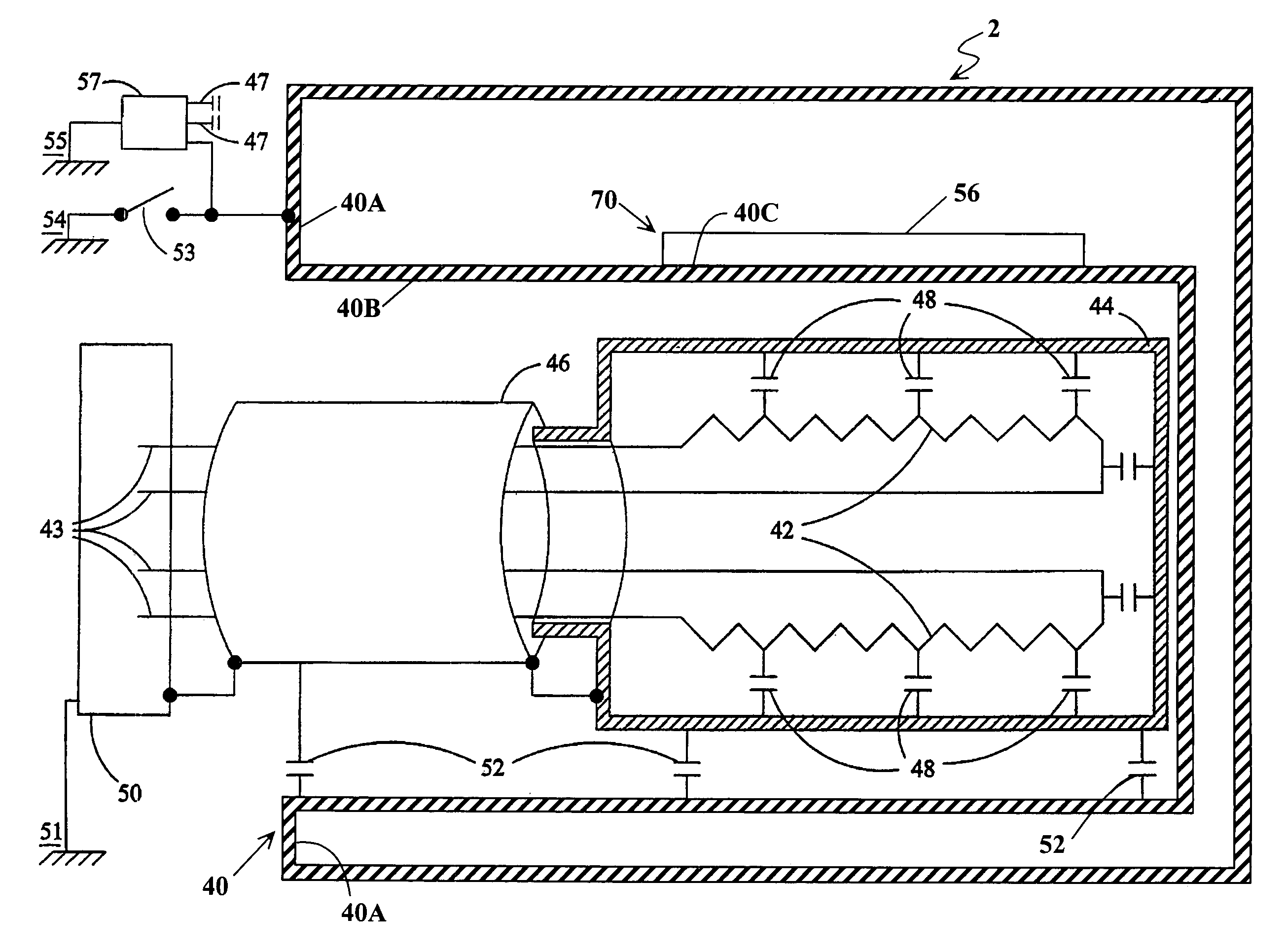
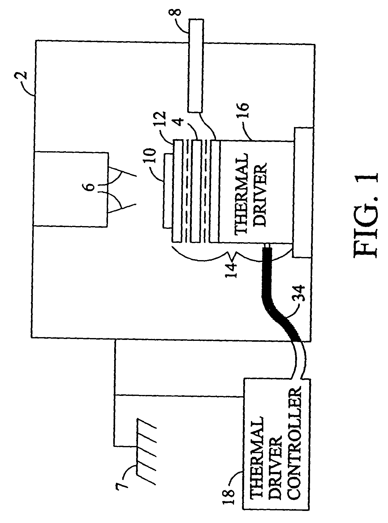
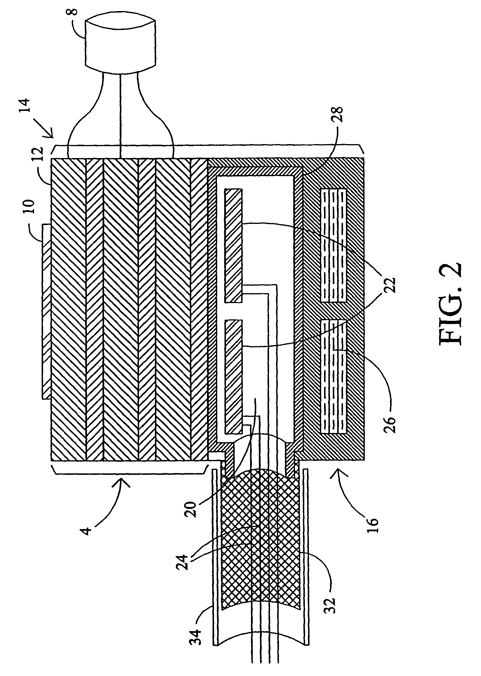
[0015]As illustrated in FIG. 1, a probe station generally includes an environmental enclosure 2 in which is located a chuck 4 and one or more probes 6. The environmental enclosure 2 is typically constructed of a conductive material and grounded 7 so that the chamber, interior to the enclosure 2, is shielded from electromagnetic fields emanating from outside of the enclosure 2. The chuck 4 typically comprises multiple layers of conductive and dielectric materials that are connected to the various conductors of a coaxial or triaxial cable 8. The chuck 4 includes a securement technique for securing a device under test 10, generally a wafer of semiconductor material, to the upper surface 12 of the chuck 4. The upper surface 12 of the chuck 4 is typically conductive. One technique for securing a device under test 10 relies on a vacuum source (not shown) located outside of the environmental enclosure. The vacuum source communicates through appropriate control valves and piping with apertu...
PUM
 Abstract
Description
Claims
Application Information