
Thin film forming method
a thin film and formation method technology, applied in the field of thin film formation method, can solve the problems of contamination particles, poor step coverage of pvd, non-even surface, etc., and achieve the effect of improving the purging
- Summary
- Abstract
- Description
- Claims
- Application Information
AI Technical Summary
Benefits of technology
Problems solved by technology
Method used
Image

Examples
embodiment 1
[0023
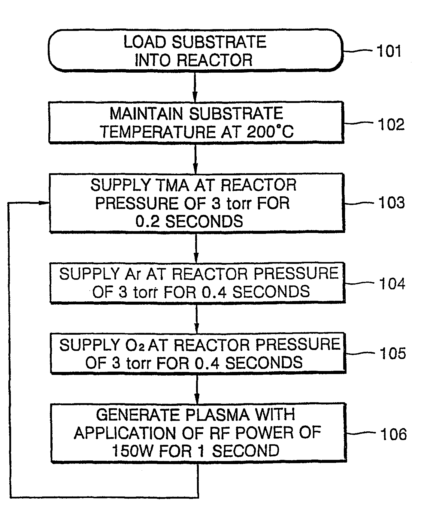
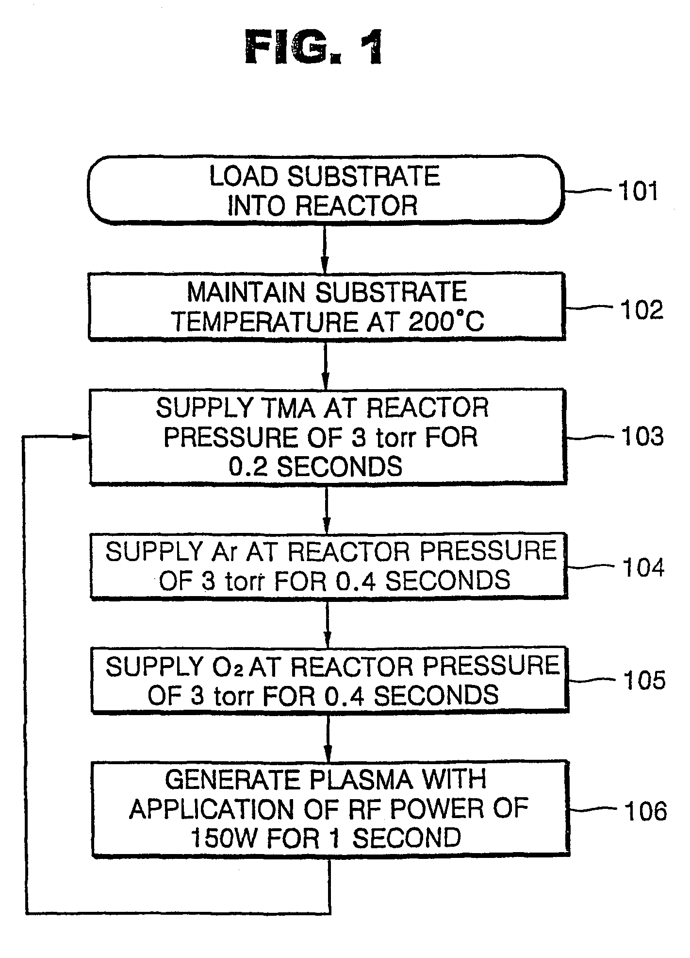
[0024]Oxygen gas (O2) reacts slowly with an organometallic source material so that it is difficult to form a metal oxide layer at a temperature of 400 EC or less with oxygen gas and an organomatallic source material. Although a metal oxide layer can be formed with oxygen gas and an organometallic source material, the film formation rate is very slow. Thus, in the present embodiment, a method of forming an aluminum oxide layer using oxygen plasma is described. FIG. 1 is a flowchart illustrating an ALD method according to a first embodiment of the present invention.
[0025]As shown in FIG. 1, an aluminum oxide (Al2O3) layer was formed using trimethylaluminum (TMA) as an aluminum source at a substrate temperature of 200 EC at a reactor pressure of 3 torr. To form the aluminum oxide layer, TMA is supplied for 0.2 seconds, argon (Ar) for 0.4 seconds, and oxygen gas (O2) for 0.4 seconds in sequence, and directly followed by oxygen plasma generation for 1 second (Step 103 through 106 of...
embodiment 2
[0028
[0029]FIG. 3 is a flowchart illustrating a second embodiment of an ALD method for forming a tantalum oxide (Ta2O5) layer according to the present invention. As shown in FIG. 3, a tantalum oxide (Ta2O5) layer was formed using dimethoxyamidoethyltetraethyltantalum (Ta(OC2H5)4(OCH2(CH2N(CH3)2), TAE(dmae)) as a tantalum source at a substrate temperature of 250 EC at a reactor pressure of 4 torr. To form the tantalum oxide layer, the sequential processing step of TAE(dmae) (0.3 sec)→Ar(1.7 sec)→O2(1 sec)→(O2+plasma)(2 sec)→Ar(1 sec) is followed, during which cycle a plasma is generated for 2 seconds with oxygen (O2) gas. This sequential pulses of gases and plasma generation totalling 6 seconds is referred to as a cycle (Step 303 through 307 of FIG. 3). Here, a radio frequency (RF) power of 180 W is applied for 2 seconds in order to generate oxygen plasma. The completion of one cycle resulted in a tantalum oxide layer having a thickness of 0.67 Å.
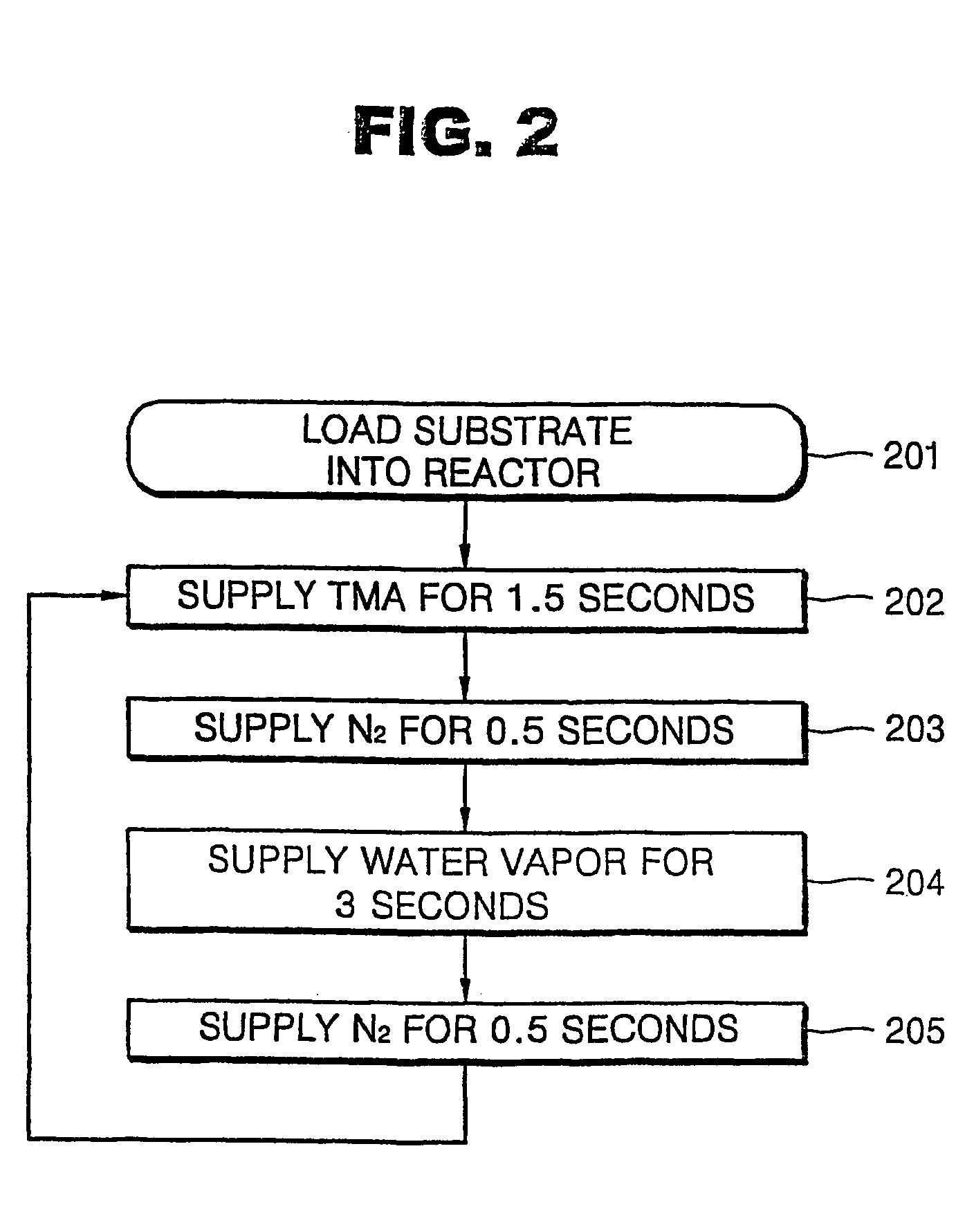
[0030]A conventional ALD method, whic...
embodiment 3
[0032
[0033]The present embodiment is directed to a plasma ALD method for forming a strontium titanate (SrTiO3; STO) layer. STO or barium strontium titanate ((Ba,Sr)TiO3; BST) has greater dielectric constant so that they are used as a dielectric material for capacitors of highly integrated memory devices such as DRAMs.
[0034]A source material Sr(thd)2, where abbreviation “thd” stands for tetramethylheptanedionate, is supplied into a reactor and then the reactor is purged with argon (Ar). Next, oxygen gas is supplied into the reactor to generate plasma and then the reactor is purged again with Ar. Ti(O-i-Pr)4 [or Ti(O-i-Pr)2(thd)2] is supplied into the reactor, and the reactor is purged again with Ar gas. Next, oxygen gas is supplied into the reactor to generate plasma and then the reactor is purged with Ar. This cycle is repeated one or more times until a STO layer having a desired thickness is obtained.
PUM
| Property | Measurement | Unit |
|---|---|---|
| pressure | aaaaa | aaaaa |
| pressure | aaaaa | aaaaa |
| time | aaaaa | aaaaa |
Abstract
Description
Claims
Application Information