
Solid-state image-pickup device with column-line amplifiers and limiters

a technology of amplifiers and limiters, which is applied in the direction of radio control devices, instruments, television systems, etc., can solve the problems of excessively high level signals, limited voltage range of constant-current sources, and complicated systems, so as to prevent the output range of amplifier elements, reduce the consumption current of amplifier elements, and maintain constant power line and ground lines

Active Publication Date: 2006-11-28
SONY CORP
View PDF4 Cites 20 Cited by
  • Summary
  • Abstract
  • Description
  • Claims
  • Application Information

AI Technical Summary

Benefits of technology

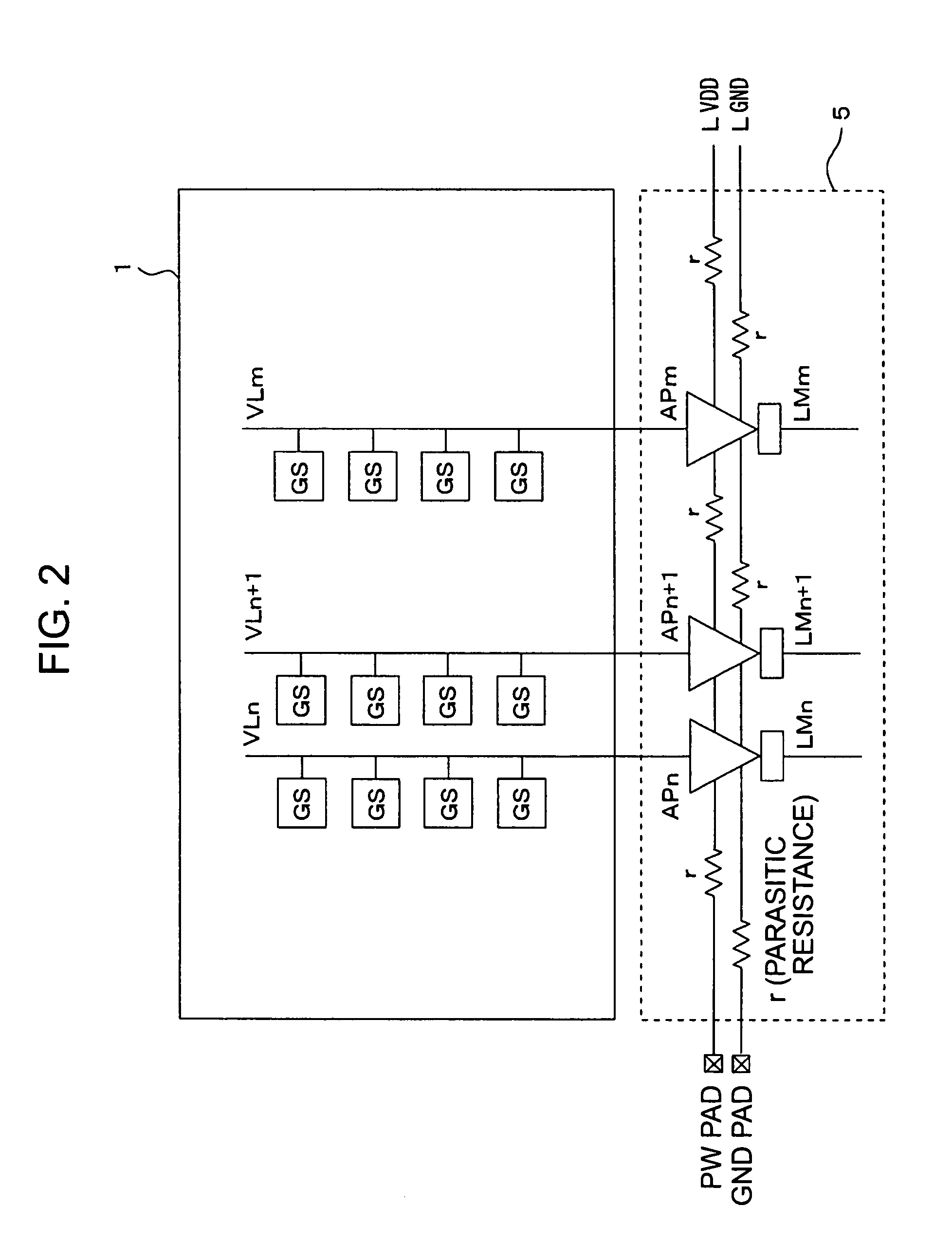
The present invention provides a solid-state image pick-up device and a pixel signal reading method that can prevent changes in the black level and horizontal stripe of the image signal caused by strong light. This is achieved by using an amplifier element with a constant current and a limiter element to limit the output voltage range of the amplifier element. The limiter element includes an MOS transistor to limit the output voltage range and ensure constant power supply and ground. The pixel signals from each column are outputted to the vertical signal line and transferred horizontally. The amplifier element includes a current source MOS transistor, a cascade MOS transistor, and an auxiliary amplifier unit to detect and keep the drain voltage constant. The invention solves the problem of changes in the power supply and ground caused by parasitic resistances and ensures a constant level of pixel signal.

Problems solved by technology

Because the CMOS image sensor solves such problems of the CCD that the manufacturing thereof needs a dedicated process, the operation needs a plurality of power voltages, and the operation requires the combination of a plurality of peripheral ICs to complicate the system.
However, the constant-current source is limited in the voltage range of the operation as the constant-current source.
An excessively-high-level signal is generated and then the output value becomes too higher.
In this case, the output voltage Vout of the amplifier is excessively high and then the current Ids via the amplifier changes.
When the current value varies depending on the amount of signals, the levels of power supply and ground change, thus causing a problem that the black level changes and the change appears in the image signal.
The appearance of stripe is a serious damage for the image sensor and becomes a problem in the case of using the single-end amplifier.

Method used


Image

  • Solid-state image-pickup device with column-line amplifiers and limiters
  • Solid-state image-pickup device with column-line amplifiers and limiters
  • Solid-state image-pickup device with column-line amplifiers and limiters

Examples


third embodiment

[0075]1. Entire common structure according to the first to third embodiment

first embodiment

[0076]2. Structure of amplifier / limiter

second embodiment

[0077]3. Structure of amplifier / limiter

[0078]4. Structure of amplifier / limiter according to the third embodiment

[0079]5. Advantages according to the first to third embodiments and modification

[0080]1. Entire Common Structure According to the First to Third Embodiment

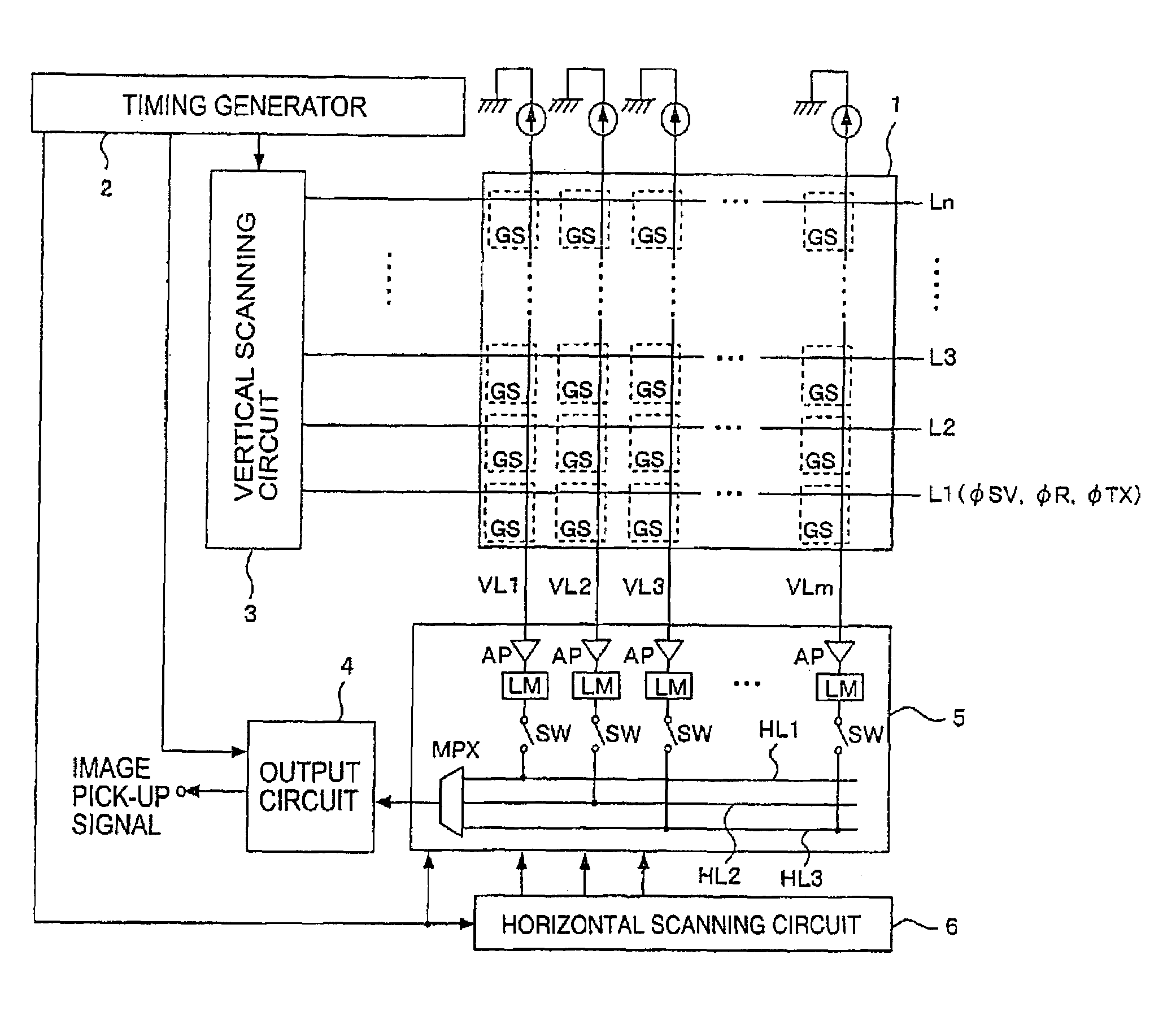
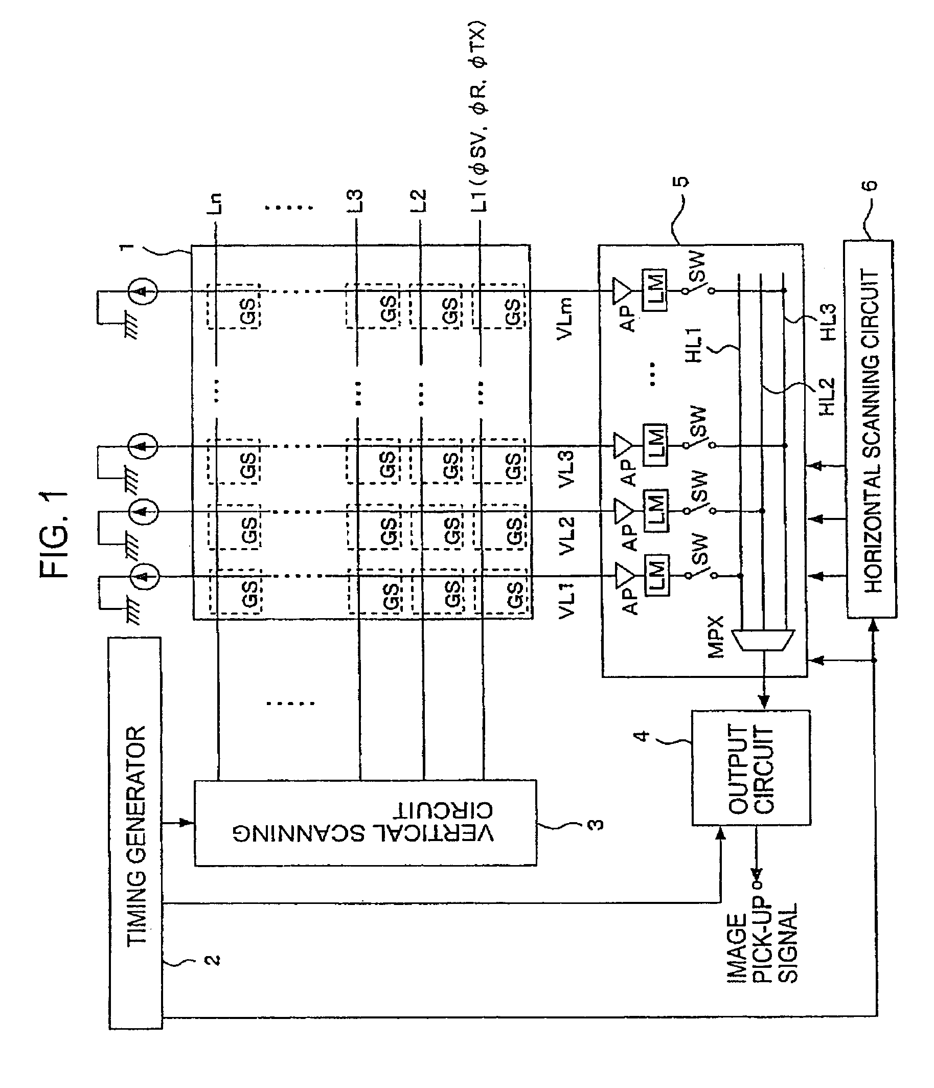
[0081]FIG. 1 is a block diagram showing a main portion of a solid-state image pick-up device according to the present invention.

[0082]Referring to FIG. 1, light from a subject is incident on a pixel array 1 via a lens system (not shown). The pixel array 1 is a CMOS sensor array, and comprises a large number of image pick-up pixels GS serving as solid-state image pick-up devices (CMOS sensors) in the row and column directions.

[0083]A vertical scanning circuit 3 selects and scans the row in the pixel array 1 based on an address and a control signal supplied from a timing generator 2. According to the present invention, the rows are sequentially scanned for selection by reading the pixel in a valid area in the column parall...


PUM


Abstract

The levels of the power supply and the ground are kept constant against a parasitic resistance by keeping the constant current of an amplifier irrespective of the size of a pixel signal and the gain of the amplifier in this case in an image signal reading circuit system having the amplifier arranged to each column. The amplifier has a limiter at an output terminal thereof which limits an output voltage of the amplifier to a range for keeping the constant consumption-current.

Description

[0001]The present application claims priority to Japanese Patent Application(s) JP2004-058621, filed in the Japanese Patent Office Mar. 3, 2004, the entire contents of which is incorporated herein by reference.BACKGROUND OF THE INVENTION[0002]1. Field of the Invention[0003]The present invention relates to a solid-state image pick-up device and a pixel signal reading method of the solid-state image pick-up device.[0004]2. Description of the Related Art[0005]Recently, a CMOS image sensor is focused as an image sensor in place of a CCD. Because the CMOS image sensor solves such problems of the CCD that the manufacturing thereof needs a dedicated process, the operation needs a plurality of power voltages, and the operation requires the combination of a plurality of peripheral ICs to complicate the system.[0006]The CMOS image sensor uses the same manufacturing process as that of a general worldwide produced CMOS integrated circuit (IC), and is driven by a single power-supply. Further, th...

Claims


Application Information

Patent Timeline
Patent Type & Authority Patents(United States)
IPC IPC(8): H01L27/00H03F3/08H04N5/335H01L27/146H01J40/14H04N25/00
CPCH04N3/155H04N5/3591H04N5/361H04N5/3658H04N5/3742H04N5/378H04N25/625H04N25/78H04N25/628H04N25/75
Inventor KOSEKI, KEN
Owner SONY CORP
Learn More