FPGA configuration memory with built-in error correction mechanism

a configuration memory and error correction technology, applied in the field of error correction, can solve problems such as design inoperativeness and value errors, and affect functions

Inactive Publication Date: 2006-11-28
XILINX INC
View PDF10 Cites 116 Cited by
  • Summary
  • Abstract
  • Description
  • Claims
  • Application Information

AI Technical Summary

Problems solved by technology

Because the functions performed by the logic or I / O blocks are determined by the values of the configuration memory cells, any error in the values could affect the functions.
In a FPGA configured to implement a complex design, it is possible that a single error could render the design inoperative.
Although the memory cells are normally very reliable, there is a concern that they might be disturbed in a high-radiation or high-temperature environment.

Method used


Image

  • FPGA configuration memory with built-in error correction mechanism
  • FPGA configuration memory with built-in error correction mechanism
  • FPGA configuration memory with built-in error correction mechanism

Examples


Embodiment Construction

[0021]The present invention relates to FPGA error detection and correction systems and methods. In the following description, numerous specific details are set forth in order to provide a more thorough understanding of the present invention. However, it will be apparent to one skilled in the art that the present invention may be practiced without these specific details. In other instances, well-known features have not been described in detail in order to avoid obscuring the present invention.

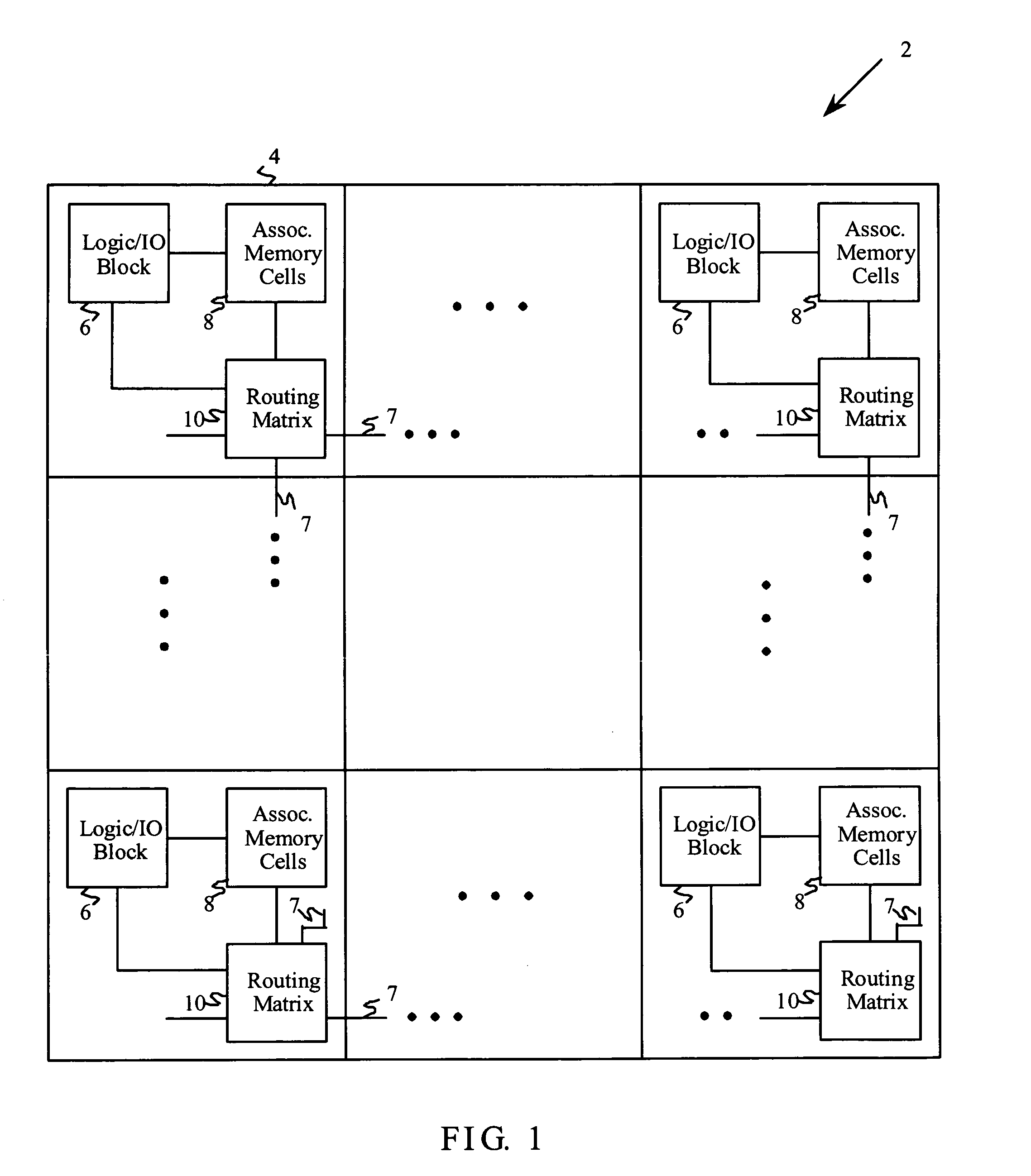
[0022]FIG. 1 shows a schematic diagram of an embodiment of an FPGA 2 on which various embodiments of the invention may be used. FPGA 2 comprises a plurality of CLBs 4. Each CLB 4 in turn comprises a logic / IO block 6, a routing matrix 10 and associated memory cell group 8. Even though FIG. 1 shows block 6, matrix 10 and memory cell group 8 as individual blocks with sharp boundary, they may be physically distributed throughout the CLB. Logic / IO block 6 is a logic and / or input-output block that can...


PUM


Abstract

A system and method are disclosed for error correction in a programmable logic device (PLD). A frame circuit retrieves data from each column of configuration memory of the PLD, and a check memory stores of a plurality of check words. A buffer circuit is coupled to the check memory and to the frame circuit. The buffer circuit assembles blocks of data from data retrieved by the frame circuit and from corresponding check words in the check memory. A plurality of storage elements are provided for storage of status information. A check circuit is coupled to the storage elements and to the buffer circuit. Each block is checked by the check circuit using an error correcting code, and data indicating detected errors is stored in the storage elements.

Description

FIELD OF THE INVENTION[0001]The present invention generally relates to error correction in programmable logic devices.BACKGROUND OF THE INVENTION[0002]Digital logic can be implemented using several options: discrete logic devices, often called small-scale integrated circuits or SSI, programmable devices such as programmable logic arrays (PLAs) or programmable logic devices (PLDs), masked-programmed gate arrays or cell-based application specific integrated circuits (ASICs), and field programmable gate arrays (FPGAs).[0003]FPGAs are general purpose programmable devices that are customized by the end users. FPGAs are composed of an array of configurable logic blocks that are programmably interconnected. The basic device architecture of an FPGA consists of an array of configurable logic blocks (CLBs) embedded in a configurable interconnect structure and surrounded by configurable I / O blocks (IOBs). An IOB allows signals to be driven off-chip or optionally brought onto the FPGA onto inte...

Claims


Application Information

Patent Timeline
Patent Type & Authority Patents(United States)
IPC IPC(8): G06F11/00G06F11/30G08C25/00H03M13/00H04L1/00
CPCG01R31/318519G06F11/1044H03K19/17764G11C7/1006G11C2029/0411
Inventor TRIMBERGER, STEPHEN M.LESEA, AUSTIN H.CURD, DEREK R.
Owner XILINX INC
Why Eureka
Try Eureka