Functional verification of logic and memory circuits with multiple asynchronous domains

a logic and memory circuit technology, applied in the field of logic and memory circuit emulation, can solve the problems of unpredictable errors, difficult and time-consuming approaches, and inability to schedule paths, and achieve the effect of convenient scheduling of paths

Active Publication Date: 2006-11-28
SIEMENS PROD LIFECYCLE MANAGEMENT SOFTWARE INC
View PDF7 Cites 37 Cited by
  • Summary
  • Abstract
  • Description
  • Claims
  • Application Information

AI Technical Summary

Benefits of technology

[0008]According to one aspect of the present invention, a method correctly transports values of an MTSD signal between a source logic module and a destination logic module by: (1) dividing the MTSD signal into related single domain signals; (2) assigning the related single domain signals to be routed through separate paths between the source and destination logic modules; and (3) causally merging the related single domain signals at the destination logic module. These logic modules can be, for example, field programmable logic arrays (FPGAs) or other programmable logic devices typically used in an emulation system. In one embodiment, the method inserts delay elements in selected paths, so that transit times in the single paths are substantially equal. In one implementation, at the destination logic module, the causal merging procedure selects as the MTSD signal value the most recently arrived value among the values on the paths. Using these techniques, correct logic operation is ensured regardless of path delays between logic modules.
[0009]In one embodiment of the present invention, a target distance is computed. That target distance has at least the l...

Problems solved by technology

However, this approach is not only difficult and time-c...

Method used


Image

  • Functional verification of logic and memory circuits with multiple asynchronous domains
  • Functional verification of logic and memory circuits with multiple asynchronous domains
  • Functional verification of logic and memory circuits with multiple asynchronous domains

Examples


Embodiment Construction

[0036]The present invention provides a method for correct functional verification of a user circuit with multiple asynchronous clock domains, using an emulation system.

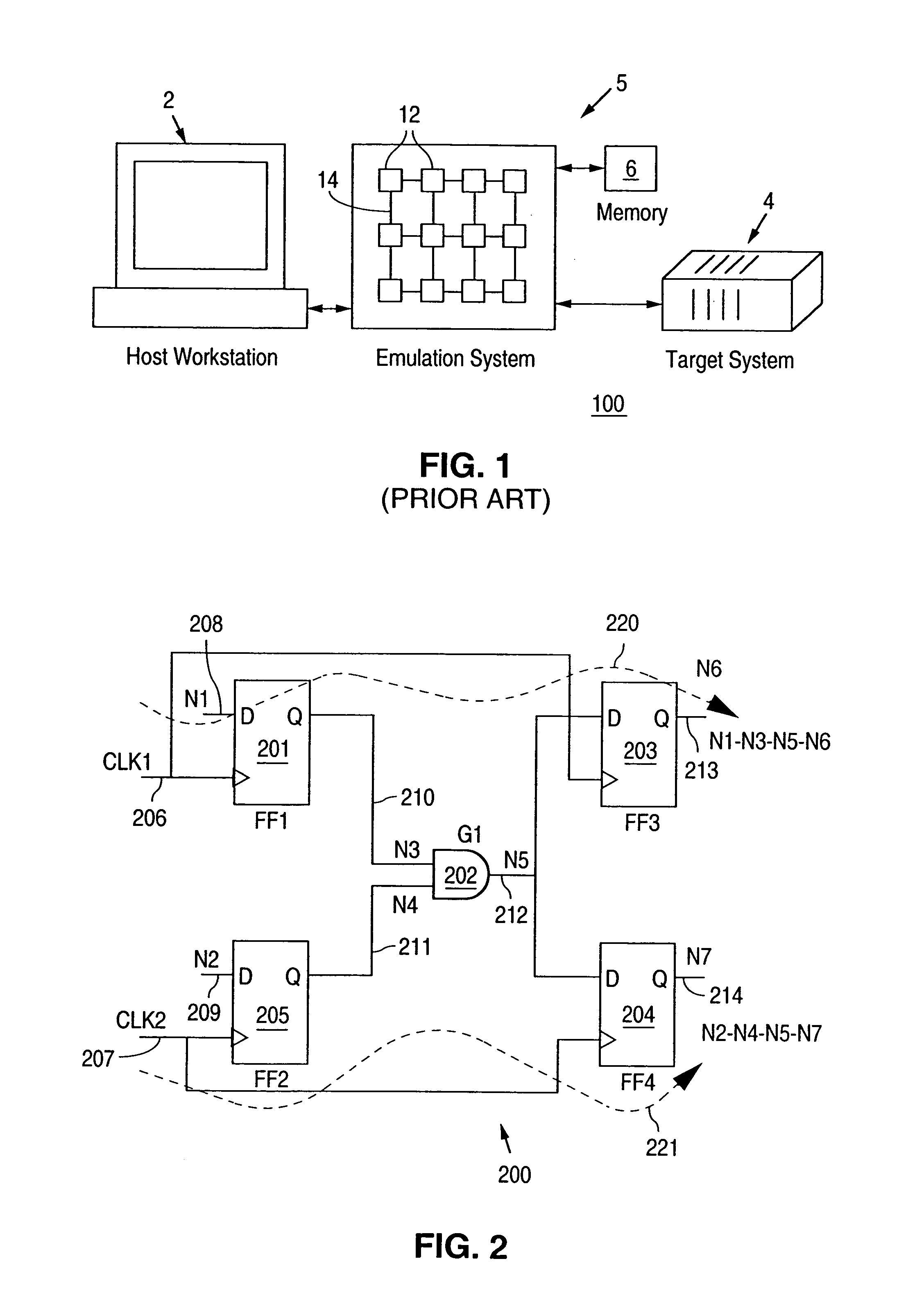
[0037]FIG. 2 shows example circuit 200 having multiple clock domains. As shown in FIG. 2, circuit 200 includes flip-flops (“FFs”) 201 and 203, which receive clock signals CLK1 at terminal 206, and FFs 204 and 205, which receive clock signal at terminal 207. Clock signals CLK1 and CLK2 are asynchronous to each other. The data output values of FFs 201 and 205 at terminals 210 and 211 are respectively input values for AND gate 202. The output value of AND gate 202 at terminal 212 is provided to the data input terminals of FFs 203 and 204. Thus, FIG. 2 includes two same-domain paths defined by (1) data input terminal 208 of FF 201, FF 201, data output terminal 210 of FF 201, gate 202, output terminal 212 of Gate 202, data input terminal of FF 203, FF 203 and data output terminal 213 of FF 203, and (2) data input terminal ...


PUM


Abstract

In an emulation system, a method is provided to schedule evaluations of state elements and memory elements receiving signals from multiple asynchronous clock domains, such that causality and hold time requirements are satisfied. In addition, a method is provided such that logic signals responsive to multiple asynchronous clock domains are transported along separate single domain path of substantially equal transit times. In one implementation, the scheduling method computes departure times and ready times for output and input terminals of logic modules, such as FPGAS.

Description

[0001]This application is a divisional application of and claims priority from application Ser. No. 10 / 103,617, filed on Mar. 20, 2002 now U.S. Pat. No. 6,817,001, of the same title.FIELD OF THE INVENTION[0002]The present invention relates to emulation of logic and memory circuits; in particular, the present invention relates to emulation of logic and memory circuits having timing signals of multiple asynchronous domains.DISCUSSION OF THE RELATED ART[0003]In logic circuit design, a logic emulation system is often used to verify the correct functional operation of a user design. One example of a logic emulation system is the field programmable gate array (FPGAs) based emulation system described in U.S. Pat. No. 5,596,742, entitled “Virtual Interconnections for Reconfigurable Systems,” issued on Jan. 21, 1997 (“Virtual Interconnection Patent”). The Virtual Interconnection Patent is hereby incorporated by reference in its entirety to provide background of the art.[0004]FIG. 1 illustrat...

Claims


Application Information

Patent Timeline
IPC IPC(8): G06F17/50
CPCG06F17/5027G06F30/331
Inventor KUDLUGI, MURALIDHAR R.SELVIDGE, CHARLES W.
Owner SIEMENS PROD LIFECYCLE MANAGEMENT SOFTWARE INC
Why Eureka
Try Eureka