Production of elemental films using a boron-containing reducing agent

a boron-containing reducing agent and elemental film technology, applied in the direction of chemical vapor deposition coating, crystal growth process, coating, etc., can solve the problems of substrate affecting the rate of deposition and difficult to obtain complete film coverage on deep vias

Inactive Publication Date: 2006-12-05
ASM INTERNATIONAL
View PDF48 Cites 303 Cited by
  • Summary
  • Abstract
  • Description
  • Claims
  • Application Information

AI Technical Summary

Problems solved by technology

This makes complete film coverage on deep vias difficult to obtain.
Additionally, the temperature of the substrate affects the rate of deposition.
While ALD has been used to produce both elemental and compound thin films, there are a number of drawbacks to the methods that have been used.

Method used


Image

  • Production of elemental films using a boron-containing reducing agent
  • Production of elemental films using a boron-containing reducing agent

Examples


example 1

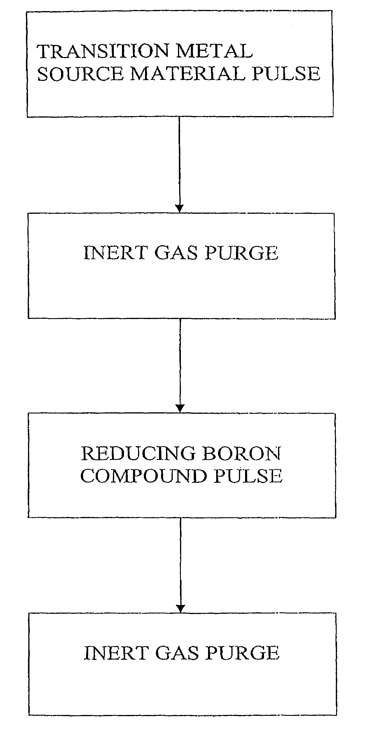
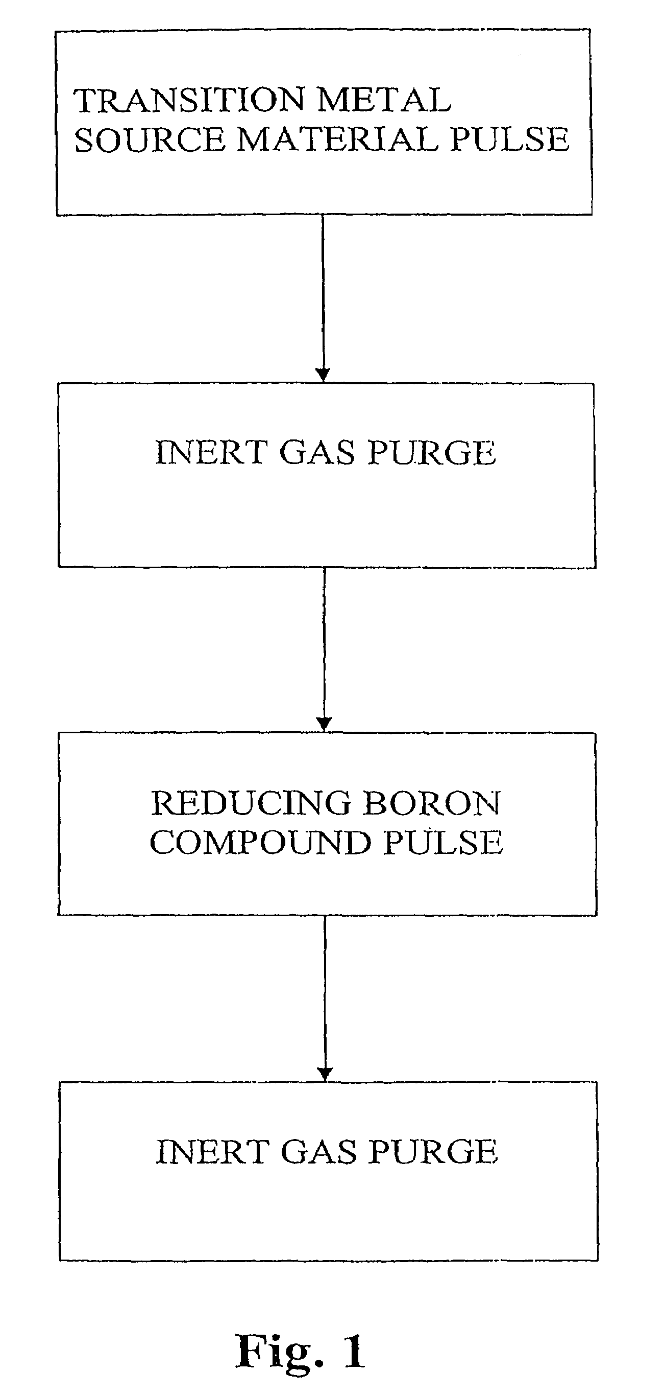
[0088]Copper chloride is pulsed into an ALD reaction chamber until heated substrate surfaces are saturated with adsorbed CuCl molecules. The substrate temperature is low enough to keep source compounds and bonds within adsorbed complex intact, but high enough to prevent condensation of CuCl. The reaction chamber is then purged with inert nitrogen gas until the surplus CuCl has been removed. TEB is then pulsed into the reaction chamber until surface reactions are complete. Examples of possible reaction equations are presented in R2 to R4. Purging the reaction chamber of any surplus TEB and reaction byproducts with inert gas completes the reaction sequence. The reaction sequence is repeated until a metal film of the desired thickness is produced. The substrate temperature is maintained low enough that the copper-copper bond formed in the adsorption of CuCl to the previous thin film layer remains intact.

[0089]A 50 mm by 50 mm piece of a silicon wafer and a 50 mm by 50 mm glass substrat...


PUM

PropertyMeasurementUnit
thicknessaaaaaaaaaa
temperatureaaaaaaaaaa

Abstract

The present invention relates generally to depositing elemental thin films. In particular, the invention concerns a method of growing elemental metal thin films by Atomic Layer Deposition (ALD) using a boron compound as a reducing agent. In a preferred embodiment the method comprises introducing vapor phase pulses of at least one metal source compound and at least one boron source compound into a reaction space that contains a substrate on which the metal thin film is to be deposited. Preferably the boron compound is capable of reducing the adsorbed portion of the metal source compound into its elemental electrical state.

Description

REFERENCE TO RELATED APPLICATIONS[0001]The present application claims the priority benefit under 35 U.S.C. § 120 as a continuation of U.S. application Ser. No. 10 / 210,715, filed Jul. 30, 2002, now U.S. Pat. No. 6,821,889, which is a continuation of U.S. application Ser. No. 09 / 687,205, filed Oct. 13, 2000, now U.S. Pat. No. 6,475,276 and under 35 U.S.C. § 119(e) to U.S. Provisional Application No. 60 / 176,948, filed Jan. 18, 2000, and No. 60 / 159,799 filed Oct. 15, 1999 and under 35 U.S.C. § 119(a) to Finnish Application Nos. FI 19992233, filed Oct. 15, 1999, FI19992234 filed Oct. 15, 1999, FI19992235, filed Oct. 15, 1999 and FI20000564, filed Mar. 10, 2000.BACKGROUND OF THE INVENTION[0002]1. Field of the Invention[0003]The present invention relates generally to a method of depositing thin films. In particular, the invention concerns a method of growing elemental metal thin films by Atomic Layer Deposition (ALD) using a boron compound as a reducing agent.[0004]2. Description of the Re...

Claims


Application Information

Patent Timeline
Patent Type & Authority Patents(United States)
IPC IPC(8): C23C16/08C23C16/02C23C16/04C23C16/32C23C16/34C23C16/44C23C16/455C30B25/02C30B25/14C30B29/02C30B29/36C30B29/38H01L21/285H01L21/768H01L23/522H01L23/532
CPCC23C16/0272C23C16/045H01L23/53295H01L23/5329H01L23/53252H01L23/53242H01L23/53238H01L23/53228C23C16/08C23C16/14C23C16/32C23C16/34C23C16/44C23C16/4401C23C16/45525C23C16/45527C23C16/45542C23C16/45553C23C16/45555C30B25/02C30B25/14C30B29/02C30B29/36C30B29/38H01L21/28562H01L21/28568H01L21/76807H01L21/76838H01L21/76843H01L21/76871H01L21/76876H01L21/76877H01L23/5226H01L23/53223H01L2924/0002H01L2924/00
Inventor ELERS, KAI-ERIKSAANILA, VILLE ANTEROKAIPIO, SARI JOHANNASOININEN, PEKKA JUHA
Owner ASM INTERNATIONAL
Why Eureka
Try Eureka