

Single cycle refresh of multi-port dynamic random access memory (DRAM)
- Summary
- Abstract
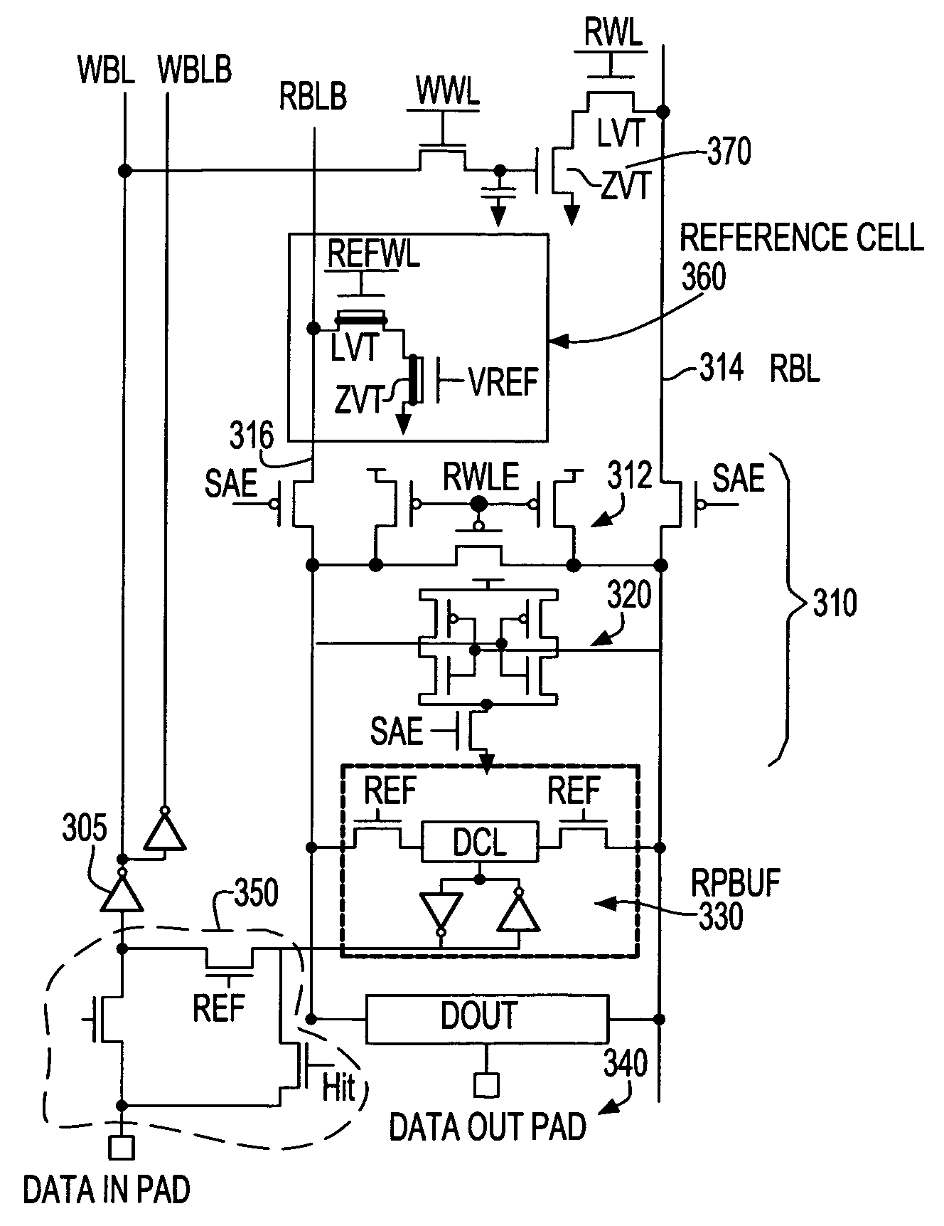
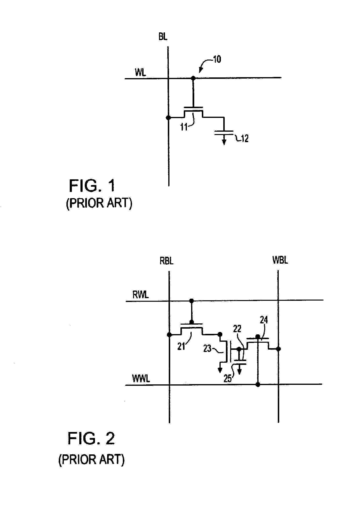
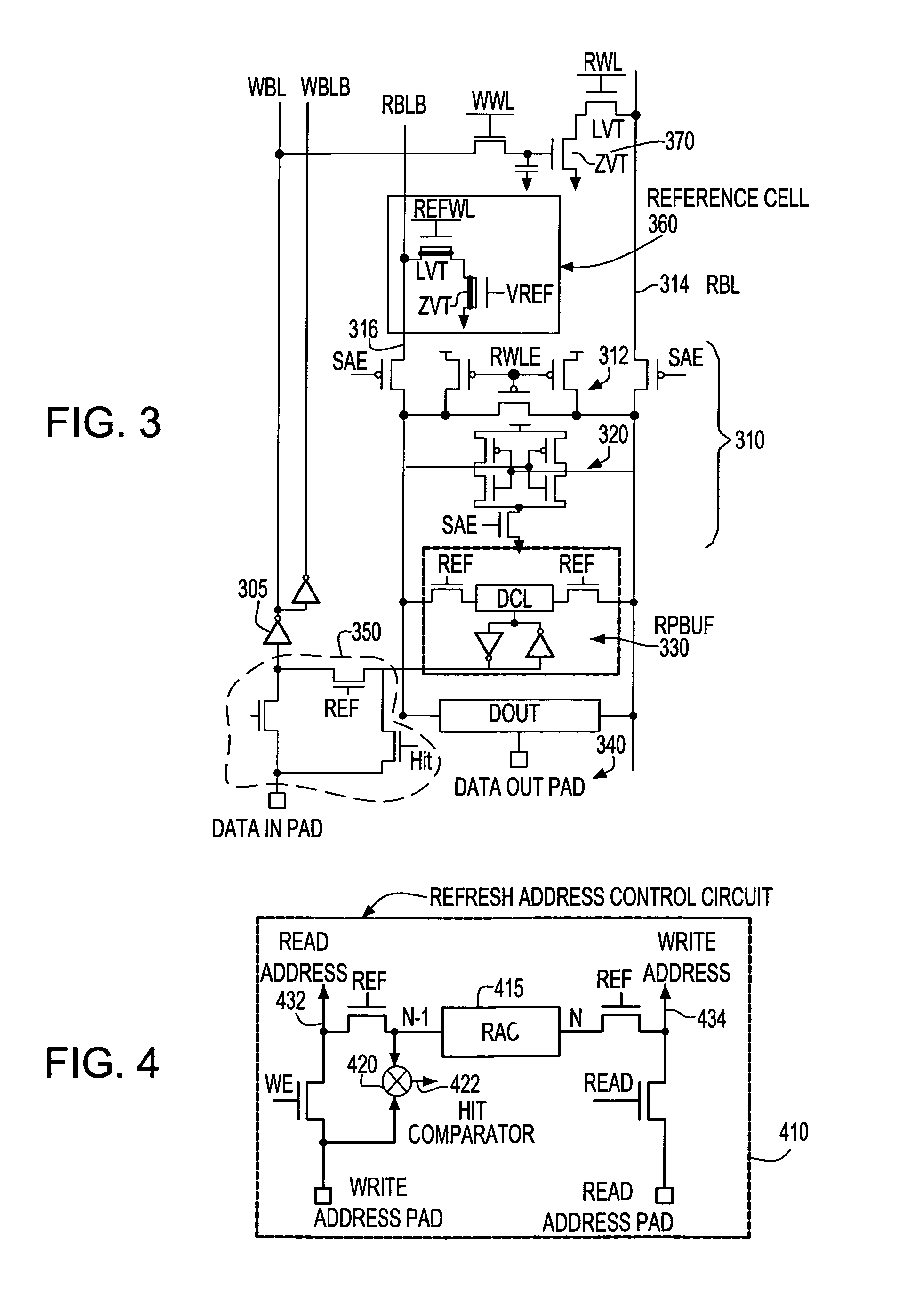
- Description
- Claims
- Application Information
AI Technical Summary
Problems solved by technology
Method used
Image

Examples
Embodiment Construction
[0014]FIG. 5 shows a set of pulse trains used with the invention that illustrates the times when the normal read and write operations and the refresh read and write operations take place.
[0015]On the top row, the CLK signals 50-1, - - - 50-5 mark off a sample of clock pulses that illustrate the operations of the system. Lines 2 and 3 show the timing of normal read and write operations to the memory. Read operations (READ), denoted with numerals 1, 3 and 5 representing read row addresses, and write operations (WE), denoted with 2, 4, 6, representing write row addresses, may both take place during the same clock cycle. Arrows extending from lines 2 and 3 to lines 5 and 6, respectively, denote that RWL and WWL are each activated within the same clock cycle as the corresponding read and write enable signals.
[0016]It is apparent on lines 5 and 6 that the refresh cycles are inserted among, the normal read and write cycles. It is also evident that the refresh cycle R1, which starts on cloc...
PUM
 Abstract
Description
Claims
Application Information