
Patterned carbon nanotube process

a carbon nanotube and cathode electron emitter technology, applied in the field of patterned carbon nanotubes, can solve the problems of low electrical current, low electrical current, and low electrical current, and achieve high electrical current, high resolution, and high resolution.

Inactive Publication Date: 2006-12-12
TECO NANOTECH CO LTD
View PDF6 Cites 11 Cited by
  • Summary
  • Abstract
  • Description
  • Claims
  • Application Information

AI Technical Summary

Benefits of technology

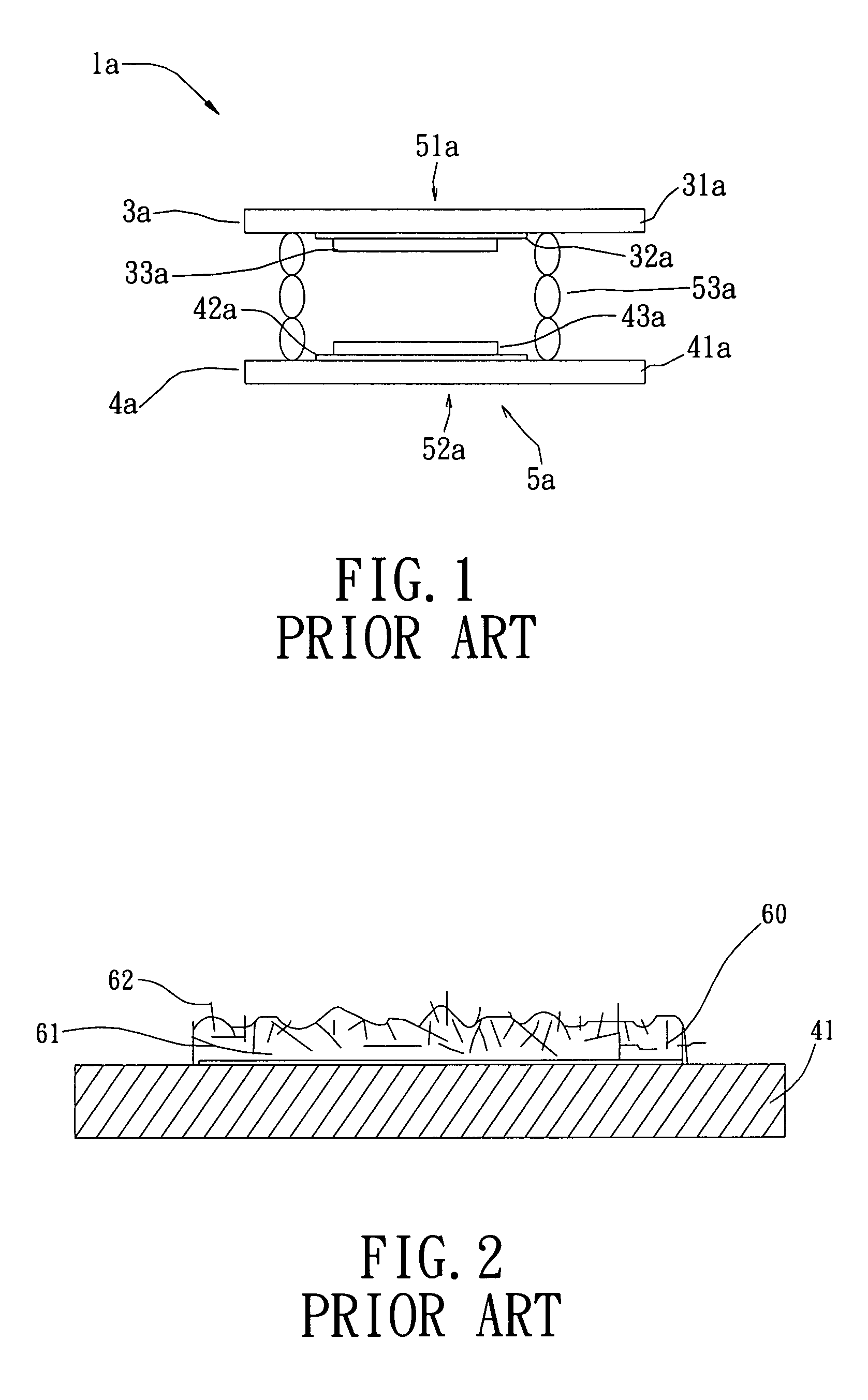
[0010]The conventional CVD process manufactures the carbon nanotubes on the cathode to provide the cathode electron emitter layer with high resolution; however, the conventional CVD process is only applicable to silicon wafers and is expensive and complicated. The screen printing process easily buries the carbon nanotubes in the paste and cannot provides a uniform height of each carbon nanotube thereby, and the electric current decreases and fails to provide the cathode electron emitter layer with high resolution. Thus, the inventor combines methods of the negative photoresist mask and the carbon nanotubes spray, which maintain high uniformity of the thickness and high electric currents, to be the cathode electron emitter layer with high resolution, and further removes the negative photoresist mask by the sintering process.
[0012]The secondary object of the invention is therefore to specify a patterned carbon nanotube process that provides easy formation and removal of a mask layer.

Problems solved by technology

The conventional CVD process manufactures the carbon nanotubes on the cathode to provide the cathode electron emitter layer with high resolution; however, the conventional CVD process is only applicable to silicon wafers and is expensive and complicated.
The screen printing process easily buries the carbon nanotubes in the paste and cannot provides a uniform height of each carbon nanotube thereby, and the electric current decreases and fails to provide the cathode electron emitter layer with high resolution.

Method used


Image

  • Patterned carbon nanotube process
  • Patterned carbon nanotube process
  • Patterned carbon nanotube process

Examples


Embodiment Construction

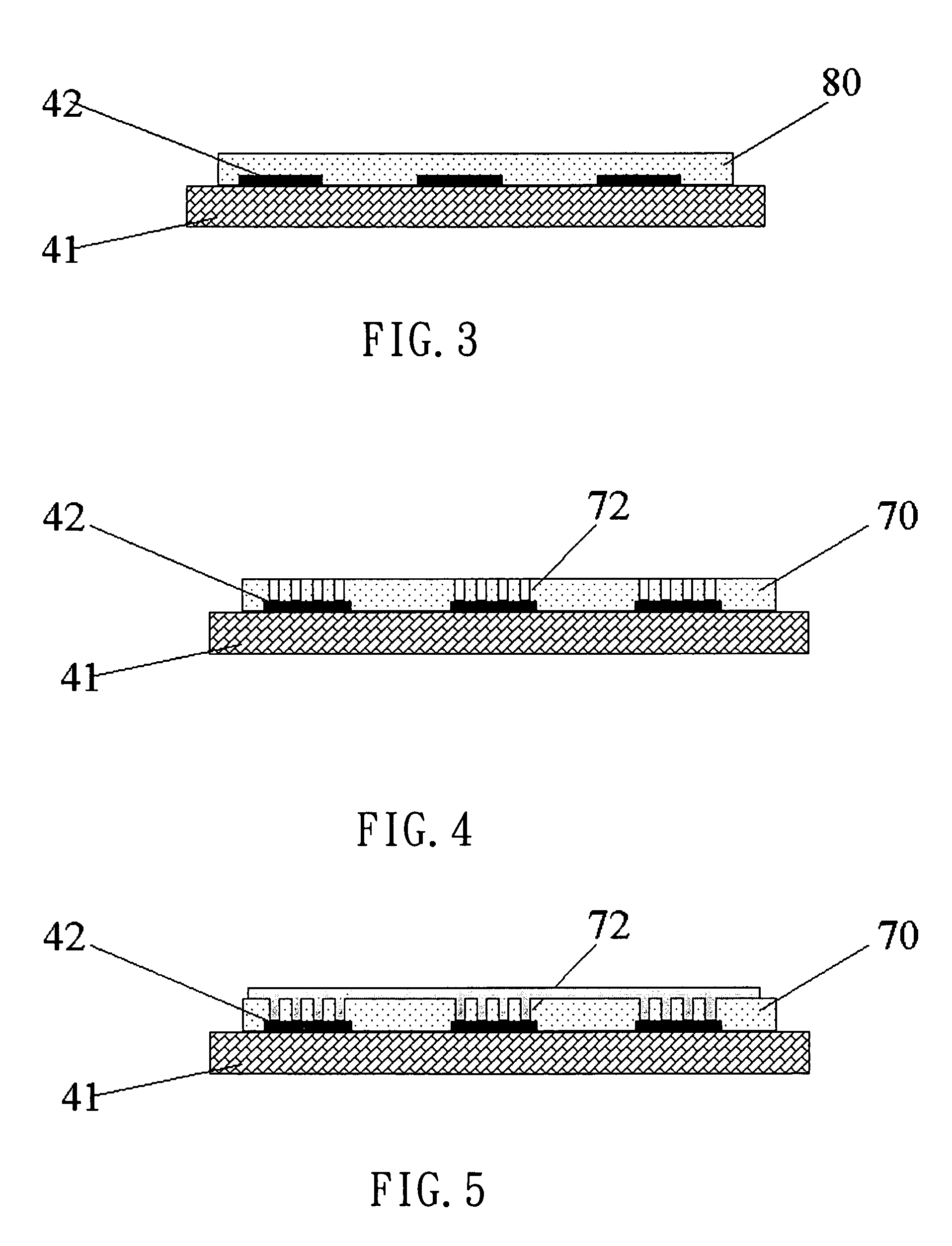
[0026]The present invention provides a patterned carbon nanotube process to make an electron emitter layer patterned with high resolution. Negative photoresist macromolecule polyester materials are provided to serve as a negative photoresist layer, and then the negative photoresist layer is sprayed with a carbon nanotube spray. The negative photoresist layer is dried out and a plurality of carbon nanotubes in the carbon nanotube spray are connected to a cathode of an electronic device in a sintering process. The carbon nanotubes patterned can provide high resolution and a thin film thereof provides a high degree of uniformity of illumination and current density.

[0027]Referring to FIGS. 3 to 7, the present invention provides negative photoresist macromolecule polyester materials or negative photoresist dry films spin-coated or printed on a cathode substrate 41 as a negative photoresist layer 80. Alternatively, the present invention provides negative photoresist dry films laminated on...


PUM

PropertyMeasurementUnit
temperatureaaaaaaaaaa
thicknessaaaaaaaaaa

Abstract

A patterned carbon nanotube process adopted for an electronic device is described. A negative photoresist layer is coated on a cathode substrate. A mask layer is formed with a carved cavity therein during a development process. A carbon nanotube spray is sprayed thereon to fill the carved cavity with a plurality of carbon nanotubes. The cathode substrate is sintered at a high temperature or in a vacuum to remove the mask layer and part of the carbon nanotubes adhered to the mask layer simultaneously, and to connect the rest of the carbon nanotubes firmly to the cathode conductive layer as an electron emitter layer with high resolution for increasing current density and uniformity of illumination of the electronic device.

Description

BACKGROUND OF THE INVENTION[0001]1. Field of the Invention[0002]The present invention relates to a technique of coating a cathode electron emitter layer a FED (Field Emission Display), and particularly relates to a method for manufacturing a cathode electron emitter layer patterned via a patterned carbon nanotube process.[0003]2. Background of the Invention[0004]A FED is a device that utilizes a cathode electron emitter to generate surrounding electrons within an electric field; the electrons excite the phosphors coated on an anode for lighting. The FED is lightweight, thin and flimsy; the effective area thereof is variable to meet requirements but without the view angle problems that occur in a flat LCD (Liquid Crystal Display).[0005]FIG. 1 shows a conventional FED 1a including a unit 5a within an anode 3a and a cathode 4a disposed therein, and a rib 53a arranged therebetween for separating the anode 3a from the cathode 4a and support. The anode 3a includes an anode glass substrate...

Claims


Application Information

Patent Timeline
Patent Type & Authority Patents(United States)
IPC IPC(8): H01J9/12B05D1/32B05D3/02B29C71/02H01J9/02H01J9/04
CPCB82Y10/00H01J9/025H01J2201/30469H01J2329/00
Inventor CHEN, SHIH-HSUNHSIAO, CHUN-YENHSIAO, SHIH-CHIENLEE, SHIE-HENGCHENG, KUEI-WEN
Owner TECO NANOTECH CO LTD
Learn More