
Read-out circuit for infrared detectors

a technology of infrared detectors and read-out circuits, which is applied in the field of infrared detector read-out circuits, can solve the problems of limiting the integration time and fixed pattern noise on the read-out circuit, and achieve the effect of low noise and high uniformity

Inactive Publication Date: 2006-12-12
XENICS
View PDF7 Cites 19 Cited by
  • Summary
  • Abstract
  • Description
  • Claims
  • Application Information

AI Technical Summary

Benefits of technology

The solution achieves reduced residual offset voltages, improved linearity, and extended integration time while maintaining low noise levels, with residual offset voltages as low as 10 μV at a 5V supply voltage, compared to 200 μV in prior art.

Problems solved by technology

In practice however such a circuit has a major drawback, namely the op-amp input voltage non-uniformity (offset), causing fixed pattern noise on the read-out circuit and limiting the integration time.

Method used


Image

  • Read-out circuit for infrared detectors
  • Read-out circuit for infrared detectors
  • Read-out circuit for infrared detectors

Examples


Embodiment Construction

[0019]The following detailed description of certain embodiments presents various descriptions of specific embodiments of the present invention. However, the present invention can be embodied in a multitude of different ways as defined and covered by the claims. In this description, reference is made to the drawings wherein like parts are designated with like numerals throughout.

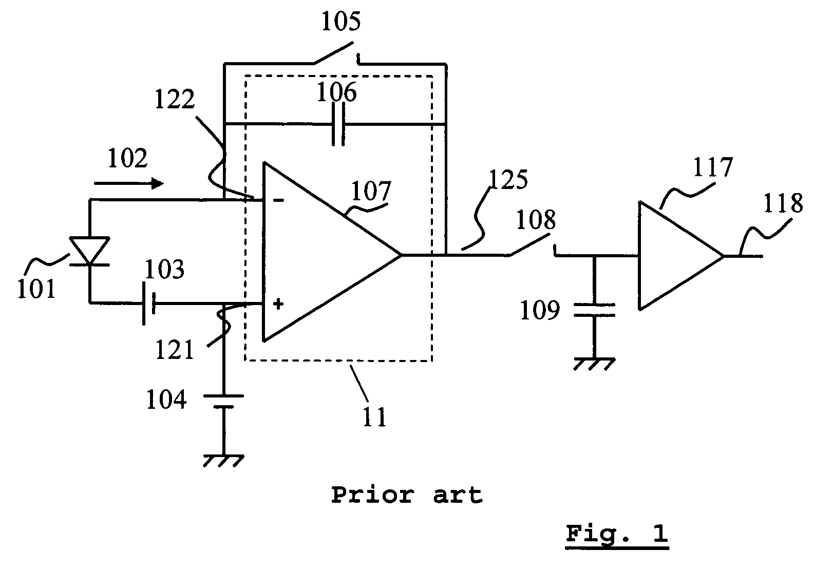
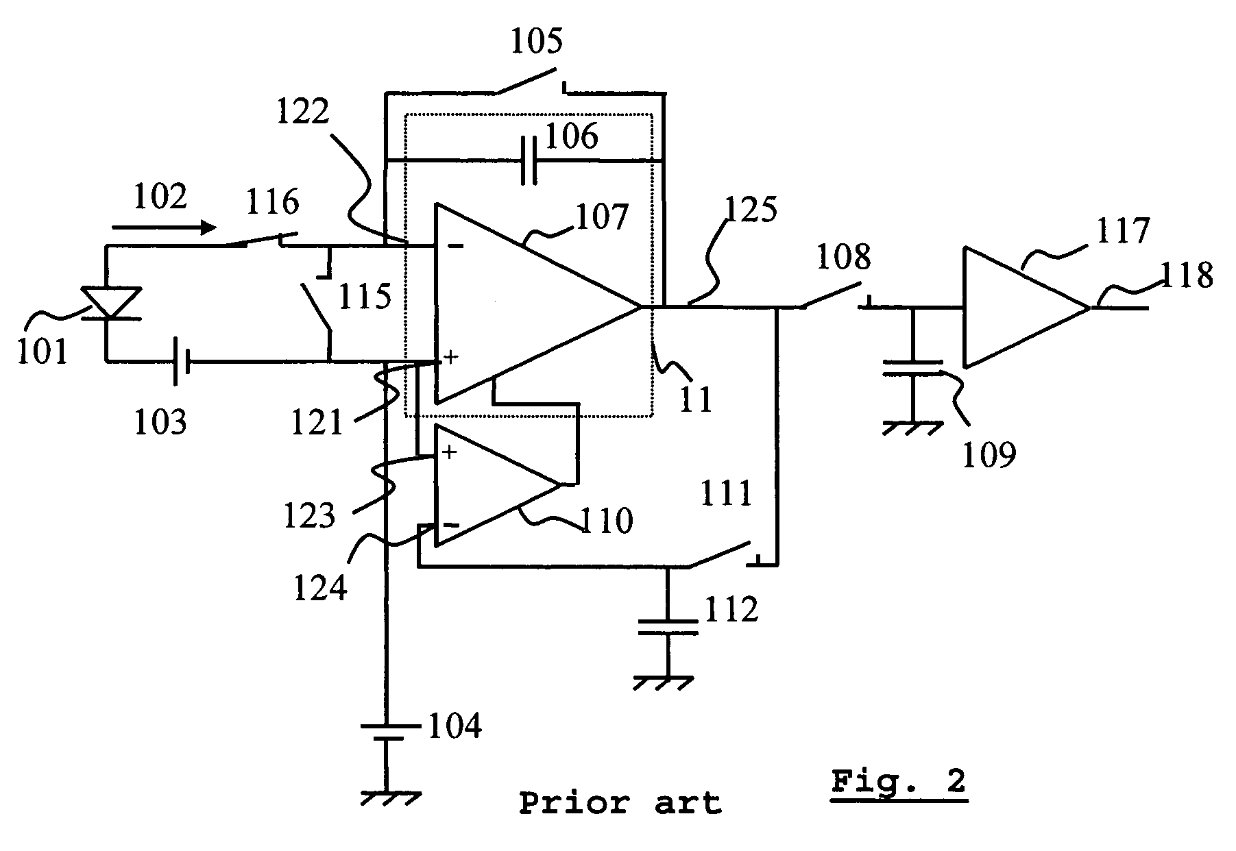
[0020]FIG. 1 shows a prior art detector buffer stage, consisting of a charge sensitive transimpedance amplifier (CTIA) (11). The CTIA accumulates all detector current 102, preferably under zero bias or some reverse bias 103 where the dynamic resistance is high. However one always has to deal with a varying offset voltage. Therefore when applying CMOS amplifiers it is common to use an auto-zero (AZ) circuit. The system exhibits an excellent linearity of the detector current 102 to output voltage conversion due to the DC coupling between the infrared detector diode 101 and the low equivalent input impedance pre...


PUM


Abstract

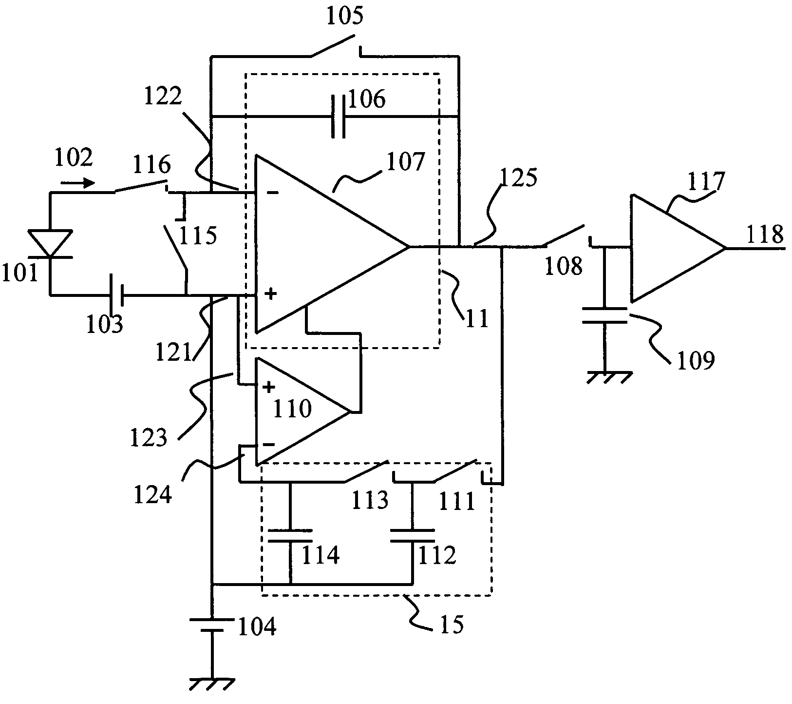
The present invention is related to a device comprising a capacitive feedback transimpedance operational amplifier, that comprises a main operational amplifier (with a first input, a second input and an output) and an integrating capacitor, connected between the second input and the output, and a first switch connected in parallel to the integrating capacitor. The device further comprises an auto-zero operational amplifier having a third input and a fourth input, whereby to the third input and the first input signals at virtual ground potential are applied. The fourth input is connected to the output by a circuit comprising two offset error capacitors, a second switch and a third switch.

Description

RELATED APPLICATIONS[0001]This is a continuation application under 35 U.S.C. § 120 of International Patent Application No. PCT / BE2003 / 00187, filed on Nov. 6, 2003 under Patent Cooperation Treaty (PCT), which was published by the International Bureau in English on May 21, 2004 as WO 04 / 043062, which designates the U.S. and claims the benefit under 35 U.S.C. § 119(e) of U.S. Provisional Patent Application No. 60 / 425,036, filed Nov. 7, 2002. The PCT Application No. PCT / BE03 / 00187 and U.S. Provisional Application No. 60 / 425,035 are hereby incorporated by reference.BACKGROUND OF THE INVENTION[0002]1. Field of the Invention[0003]The present invention is related to low offset, low noise auto-zeroed CMOS integrated circuit amplifiers and more in particular to read-out circuits for infrared detectors.[0004]2. Description of the Related Art[0005]A focal plane array comprises several individual detector elements (pixels). The number of pixels in a linear or focal plane array is increasing. The...

Claims


Application Information

Patent Timeline
Patent Type & Authority Patents(United States)
IPC IPC(8): H03K5/22H03D13/00H03F3/08H03F3/45H04N5/217H04N5/33
CPCH03F3/087H03F3/45977H04N5/33H04N5/3651H03F2200/261H04N25/671H04N23/20
Inventor VAN BOGGET, URBAIN
Owner XENICS
Learn More