Silver-selenide/chalcogenide glass stack for resistance variable memory

a technology of resistance variable and chalcogenide glass, which is applied in the direction of digital storage, radio frequency controlled devices, instruments, etc., can solve the problems of volatile ram devices, loss of stored data, shrinking of the size of each element,

Inactive Publication Date: 2006-12-19
MICRON TECH INC
View PDF86 Cites 103 Cited by
  • Summary
  • Abstract
  • Description
  • Claims
  • Application Information

AI Technical Summary

Benefits of technology

[0011]In a first embodiment, the invention provides a resistance variable memory element and a method of forming the resistance variable memory element in which a metal containing layer is formed betwe

Problems solved by technology

Typically, RAM devices are volatile, in that stored data is lost once the power source is disconnected or removed.
Accordingly, the size of each element has been shrinking, which in the case of DRAMs also shortens the element's data holding time.
However, with increasing element number and density, it is becoming more and more difficult to refresh a

Method used


Image

  • Silver-selenide/chalcogenide glass stack for resistance variable memory
  • Silver-selenide/chalcogenide glass stack for resistance variable memory
  • Silver-selenide/chalcogenide glass stack for resistance variable memory

Examples


first embodiment

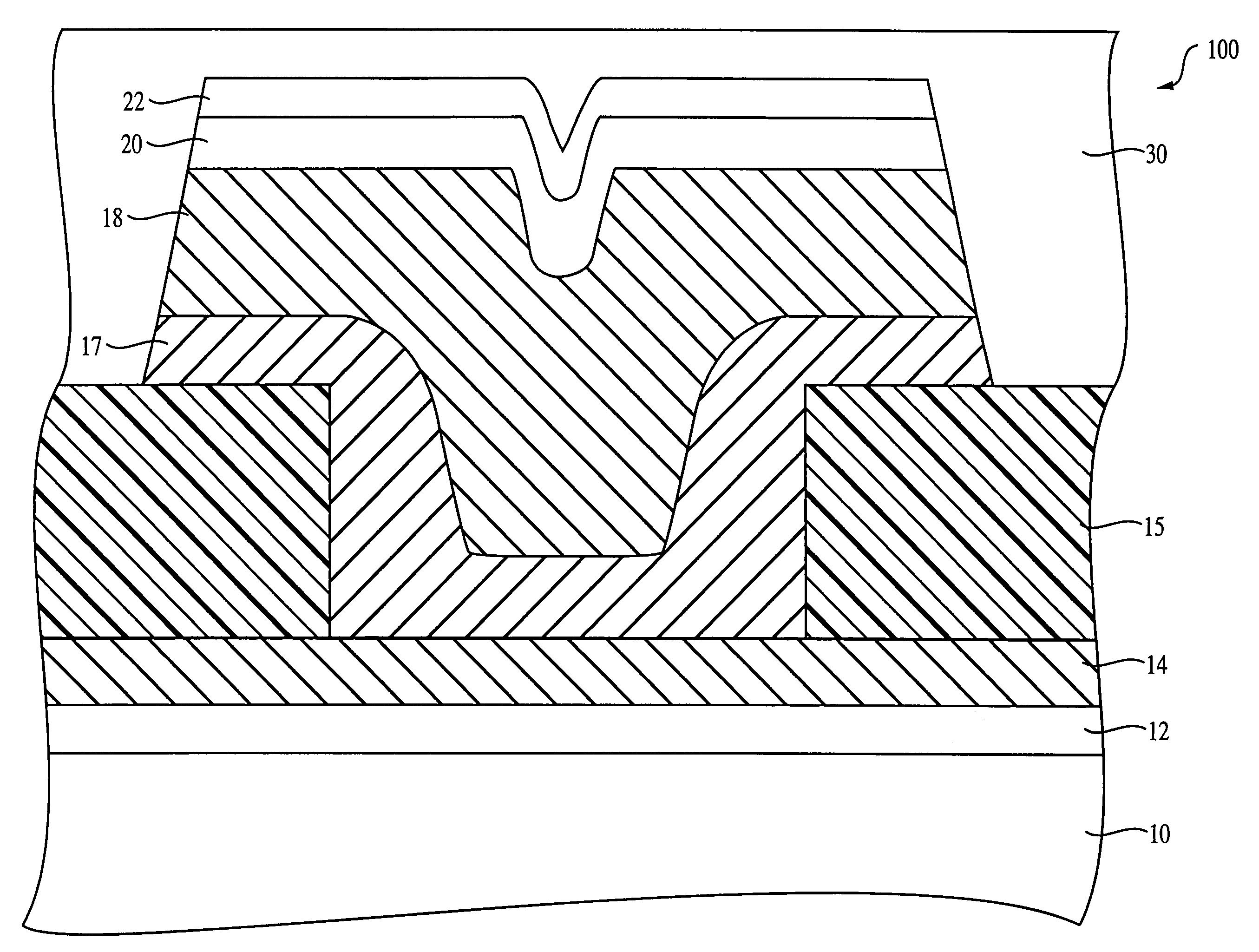
[0037]According to the invention, the first chalcogenide glass layer 17 is a germanium-selenide glass having a GexSel100−x stoichiometry. The preferred stoichiometric range is between about Ge20Se80 to about Ge43Se57 and is more preferably about Ge40Se60. The first chalcogenide glass layer 17 preferably has a thickness from about 100 Å to about 1000 Å and is more preferably 150 Å.

[0038]The first chalcogenide glass layer, acts as a glass backbone for allowing a metal containing layer, such as a silver-selenide layer, to be directly deposited thereon. The use of a metal containing layer, such as a silver-selenide layer, in contact with the chalcogenide glass layer makes it unnecessary to provide a metal (silver) doped chalcogenide glass, which would require photodoping of the substrate with ultraviolet radiation. However, it is possible to also metal (silver) dope the chalcogenide glass layer, which is in contact with the silver-selenide layer, as an optional variant.

[0039]The formati...

second embodiment

[0052]Referring now to FIG. 9, which shows the invention subsequent to the processing step shown in FIG. 4, the stack of layers formed between the first and second electrodes may include alternating layers of chalcogenide glass and a metal containing layer such as a silver-selenide layer. As shown in FIG. 9, a first chalcogenide glass layer 17 is stacked atop a first electrode 14, a first silver-selenide layer 18 is stacked atop the first chalcogenide glass layer 17, a second chalcogenide glass layer 117 is stacked atop the first silver-selenide layer 18, a second silver-selenide layer 118 is stacked atop the second chalcogenide glass layer 117, a third chalcogenide glass layer 217 is stacked atop the second silver-selenide layer 118, a third silver-selenide layer 218 is stacked atop the third chalcogenide glass layer 217, and a fourth chalcogenide glass layer is stacked atop the third silver-selenide layer 218. The second conductive electrode 22 is formed over the fourth chalcogeni...


PUM


Abstract

The invention is related to methods and apparatus for providing a resistance variable memory element with improved data retention and switching characteristics. According to an embodiment of the invention a resistance variable memory element is provided having at least one silver-selenide layer in between glass layers, wherein at least one of the glass layers is a chalcogenide glass, preferably having a GexSe100−x composition.

Description

[0001]This application is a continuation of U.S. patent application Ser. No. 10 / 077,867, filed Feb. 20, 2002 (now abandoned), the entirety of which is hereby incorporated by reference.FIELD OF THE INVENTION[0002]The invention relates to the field of random access memory (RAM) devices formed using a resistance variable material, and in particular to a resistance variable memory element formed using chalcogenide glass.BACKGROUND OF THE INVENTION[0003]A well known semiconductor component is semiconductor memory, such as a random access memory (RAM). RAM permits repeated read and write operations on memory elements. Typically, RAM devices are volatile, in that stored data is lost once the power source is disconnected or removed. Non-limiting examples of RAM devices include dynamic random access memory (DRAM), synchronized dynamic random access memory (SDRAM) and static random access memory (SRAM). In addition, DRAMS and SDRAMS also typically store data in capacitors which require period...

Claims


Application Information

Patent Timeline
IPC IPC(8): H01L29/04H01L27/105G11C11/34G11C13/02H01L21/20H01L27/10H01L27/148H01L27/24H01L45/00
CPCG11C13/0011H01L45/1625H01L45/1233H01L45/143H01L45/1616H01L45/085G11C2213/51G11C2213/56H10N70/245H10N70/8825H10N70/023H10N70/026H10N70/826H01L27/10
Inventor CAMPBELL, KRISTY A.MOORE, JOHN T.
Owner MICRON TECH INC
Why Eureka
Try Eureka