Memory system and data transmission method

a memory system and data transmission technology, applied in the field of memory systems, can solve the problems of speedup and the limitation of the number of memory modules that can be mounted, and achieve the effect of easy adjustment of timing between data signals

Active Publication Date: 2006-12-26
LONGITUDE LICENSING LTD
View PDF19 Cites 92 Cited by
  • Summary
  • Abstract
  • Description
  • Claims
  • Application Information

AI Technical Summary

Benefits of technology

[0013]Therefore, it is an object of the present invention to provide a memory system that can easily adjust timing between data signals, and command / address and clock signals in each memory module.
[0014]It is another object of the present invention to provide a memory system that can reduce reflection signals caused by branching and impedance mismatching and, as a result, that can operate at high speed.
[0015]It is still another object of the present invention to provide a data transfer method that can transfer data at high speed between two circuits provided in a module.

Problems solved by technology

Therefore, data arrives at each DRAM at timing that differs from arrival timing of command / address and clock signals, and thus, it is difficult to adjust the timing therebetween.
Further, in the configuration of Reference 2, since the transfer speed of data can not exceed the operation speed of the memory, there arises a limitation about the speedup and the number of memory modules that can be mounted.

Method used


Image

  • Memory system and data transmission method
  • Memory system and data transmission method
  • Memory system and data transmission method

Examples


Embodiment Construction

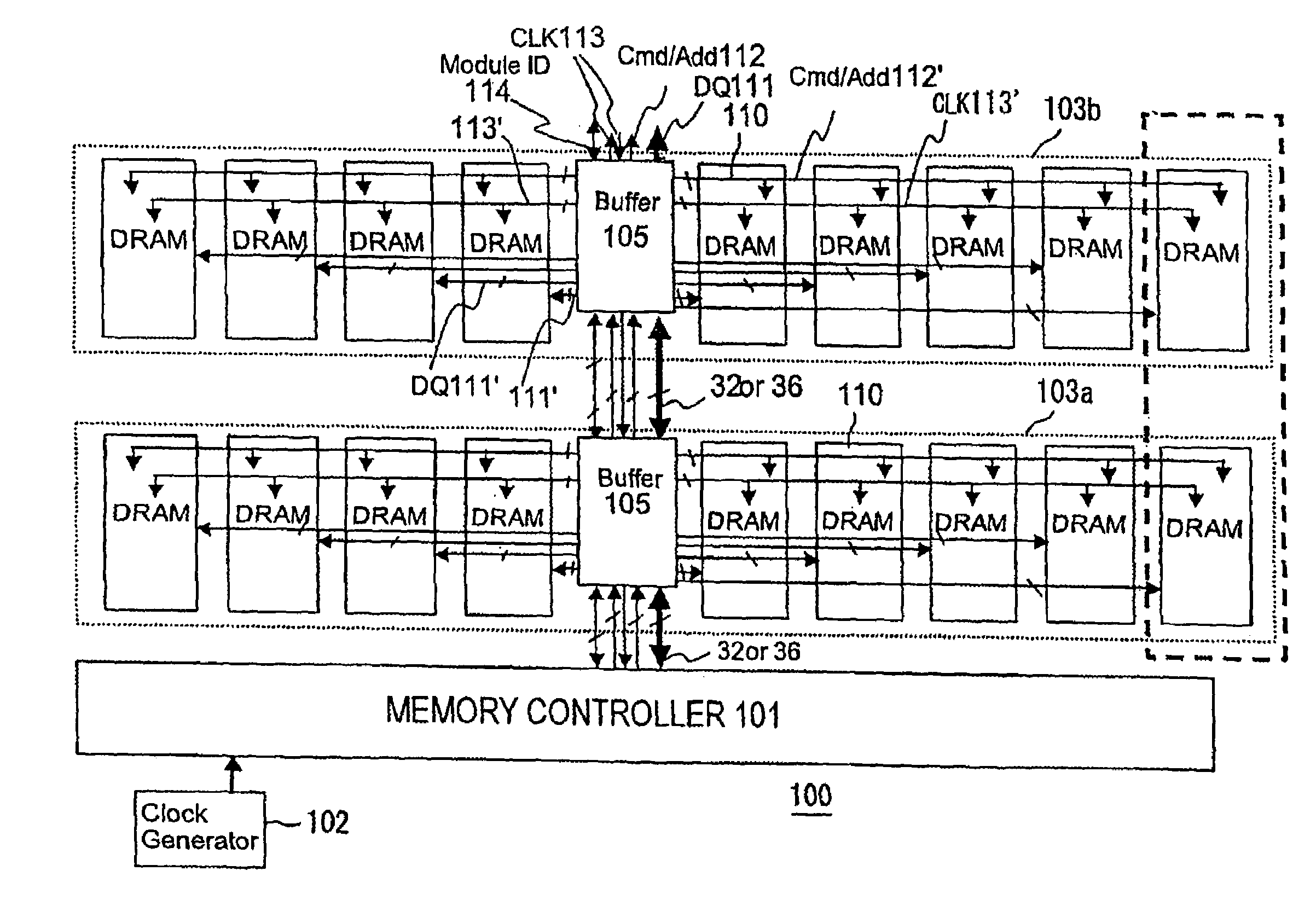
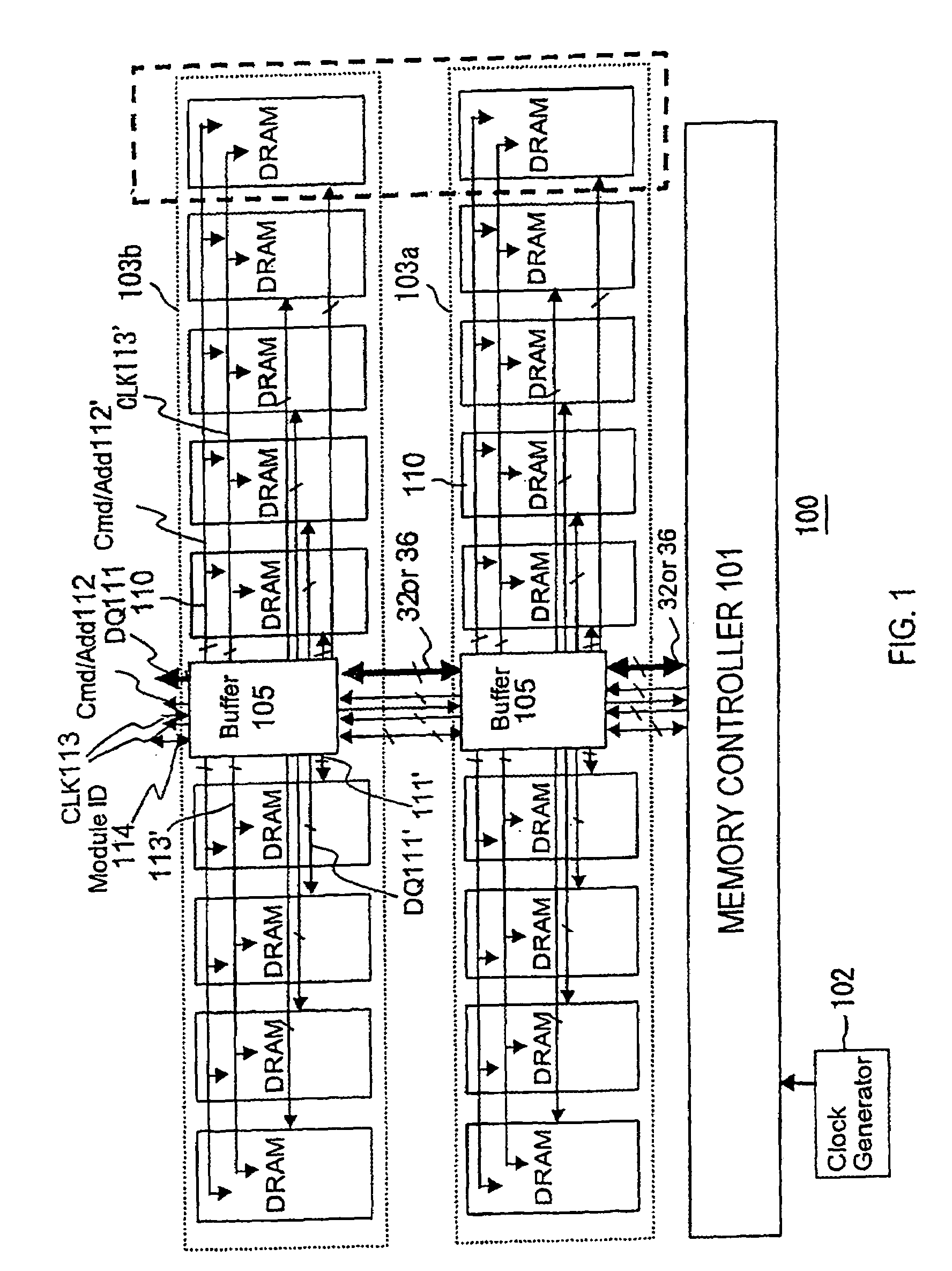
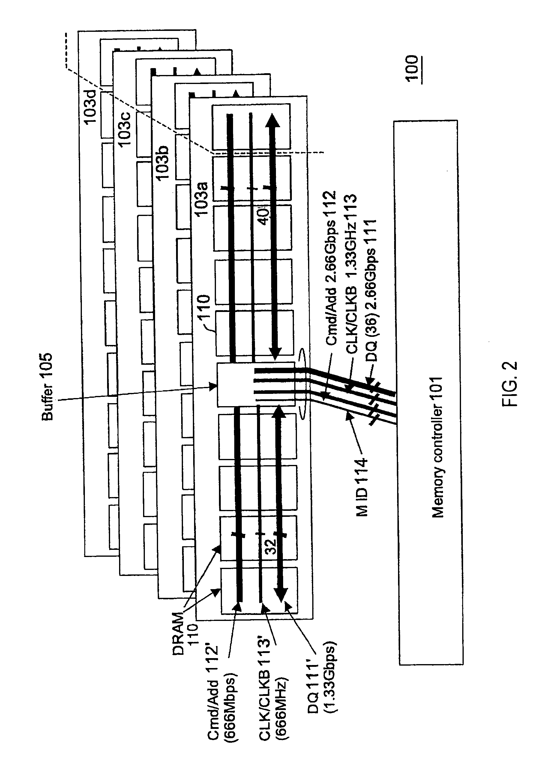
[0135]Referring to FIGS. 1 and 2, there are respectively shown a wiring diagram and a stereoscopic diagram of a memory system according to a first preferred embodiment of the present invention. Further, FIG. 3 is a partial sectional view of the memory system for explaining the wiring at a portion of FIGS. 1 and 2 in detail.

[0136]As seen from the figures, the memory system according to the first preferred embodiment of the present invention comprises a memory controller 101 and a clock generator 102 (FIG. 1) that are mounted on a mother board 100. Further, on the mother board 100, a plurality of memory modules 103 (four memory modules 103a, 103b, 103c, and 103d in FIGS. 2 and 3) are mounted via module connectors 104 (FIG. 3).

[0137]Each memory module 103 (subscript omitted) is provided on a module board thereof with a buffer 105 and, as shown in FIGS. 1 and 2, a plurality of DRAMs 110. In the shown example, each memory module 103 has one buffer 105, and the memory controller 101 and t...


PUM


Abstract

A memory system of a high-speed operation can be realized by reducing an influence of reflection signals etc. caused by branching and impedance mismatching in various wirings between a memory controller and a memory module, and an influence due to transmission delays of data, command / address, and clocks in the memory module. To this end, a memory system comprises a memory controller and a memory module mounted with DRAMs. A buffer is mounted on the memory module. The buffer and the memory controller are connected to each other via data wiring, command / address wiring, and clock wiring. The DRAMs and the buffer on the memory module are connected to each other via internal data wiring, internal command / address wiring, and internal cock wiring. The data wiring, the command / address wiring, and the clock wiring may be connected to buffers of other memory modules in cascade. Between the DRAMs and the buffer on the memory module, high-speed data transmission is implemented using data phase signals synchronous with clocks.

Description

BACKGROUND OF THE INVENTION[0001]1. Field of the Invention[0002]The present invention relates to a memory system having a configuration that enables high-speed operation, and further relates to a data transmission system that is used in the memory system.[0003]2. Description of the Related Art[0004]Conventionally, in the memory systems of this type, interfaces have been studies that enable operations at high speed and with low signal amplitude. As a standard for such interfaces, SSTL (Stub Series Terminated Transceiver Logic) has been proposed. Further, with respect to the memory systems having DRAMs as memory devices, there have been proposed such memory systems employing a DDR (Double Data Rate) system wherein a data transmission speed can be twice by inputting / outputting data synchronously with both edges of rise (leading edge) and fall (trailing edge) of clocks, thereby to operate the DRAMs at high speed.[0005]Conventionally, as a memory system employing the foregoing SSTL and D...

Claims


Application Information

Patent Timeline
Patent Type & Authority Patents(United States)
IPC IPC(8): G06F13/14G06F1/18G06F12/00G06F12/06G06F13/16G06F13/38G06F13/42G11C7/00G11C7/10G11C11/401G11C11/4093
CPCG06F13/4243G06F13/4256G11C7/10G11C8/18G11C29/028G11C29/50012G11C7/1048G11C11/4093G11C11/401G11C11/4082G11C11/4076G11C7/1057G11C5/04G11C5/063G11C7/1084G11C7/1072G11C7/222G11C7/1093G11C7/1066G11C7/109G11C29/023G11C7/00
Inventor MATSUI, YOSHINORI
Owner LONGITUDE LICENSING LTD
Why Eureka
Try Eureka