Clock controller for at-speed testing of scan circuits

a clock controller and scan circuit technology, applied in the field of integrated circuit testing, can solve the problems of patent disclosure of how to perform an at-speed test of all clock domains, inability to test complex failure mechanisms with short bursts, and inability to test complex failure mechanisms

Active Publication Date: 2006-12-26
SIEMENS PROD LIFECYCLE MANAGEMENT SOFTWARE INC
View PDF13 Cites 31 Cited by
  • Summary
  • Abstract
  • Description
  • Claims
  • Application Information

AI Technical Summary

Benefits of technology

[0011]Another aspect of the present invention is generally defined as An at-speed scan test method for testing a circuit having of interacting synchronous clock domains, the method having a shift phase for loading test patterns into scan chains in the clock domains and unloading test response patterns from the scan chains, and a burst phase for launching test patterns and capturing circuit responses to the test patterns. The method comprises generating a burst phase signal following the shift phase; synchronizing the burst phase signal with a reference clock associated with the clock domain having the lowest clock frequency; and, for each clock domain: generating a burst of clock cycles derived from a reference clock signal associated with the clock domain; and, prior to the generating a burst of clock cycles, delaying commencement of the burst of clock cycles by a predetermined time interval so as to align a selected edge of the burst of clock cycles with a corresponding edge in all other interacting synchronous clock domains.

Problems solved by technology

Short bursts are not appropriate to test for complex failure mechanisms such as power supply noise, IR-drop, signal coupling, etc .
The size of the registers become prohibitive for long burst lengths.
The patent does not disclose how to perform an at-speed test of all clock domains at the same time if the clocks are not multiples of each other because all capture clocks are derived from a single capture clock source.
Further, the patent does not specifically address how to handle interacting synchronous clock domains and the disclosed method applies only to the Level Sensitive Scan Design (LSSD) style.

Method used


Image

  • Clock controller for at-speed testing of scan circuits
  • Clock controller for at-speed testing of scan circuits
  • Clock controller for at-speed testing of scan circuits

Examples


Embodiment Construction

[0021]In the following detailed description, numerous specific details are set forth in order to provide a thorough understanding of the present invention, However, it will be understood by those skilled in the art that the present invention may be practiced without these specific details. In other instances, well known methods, procedures, components and circuits have not been described in detail so as not to obscure aspects of the present invention.

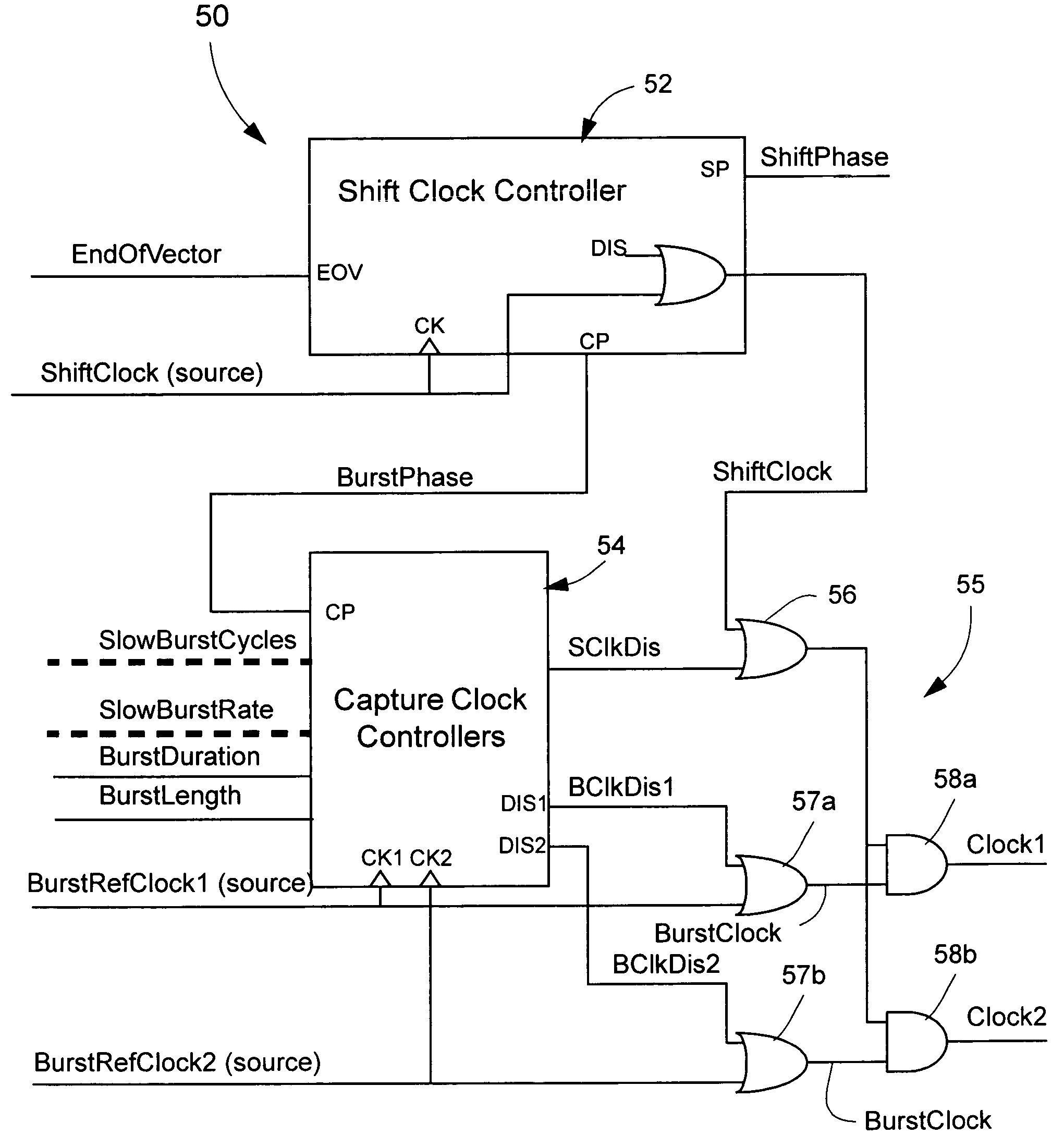
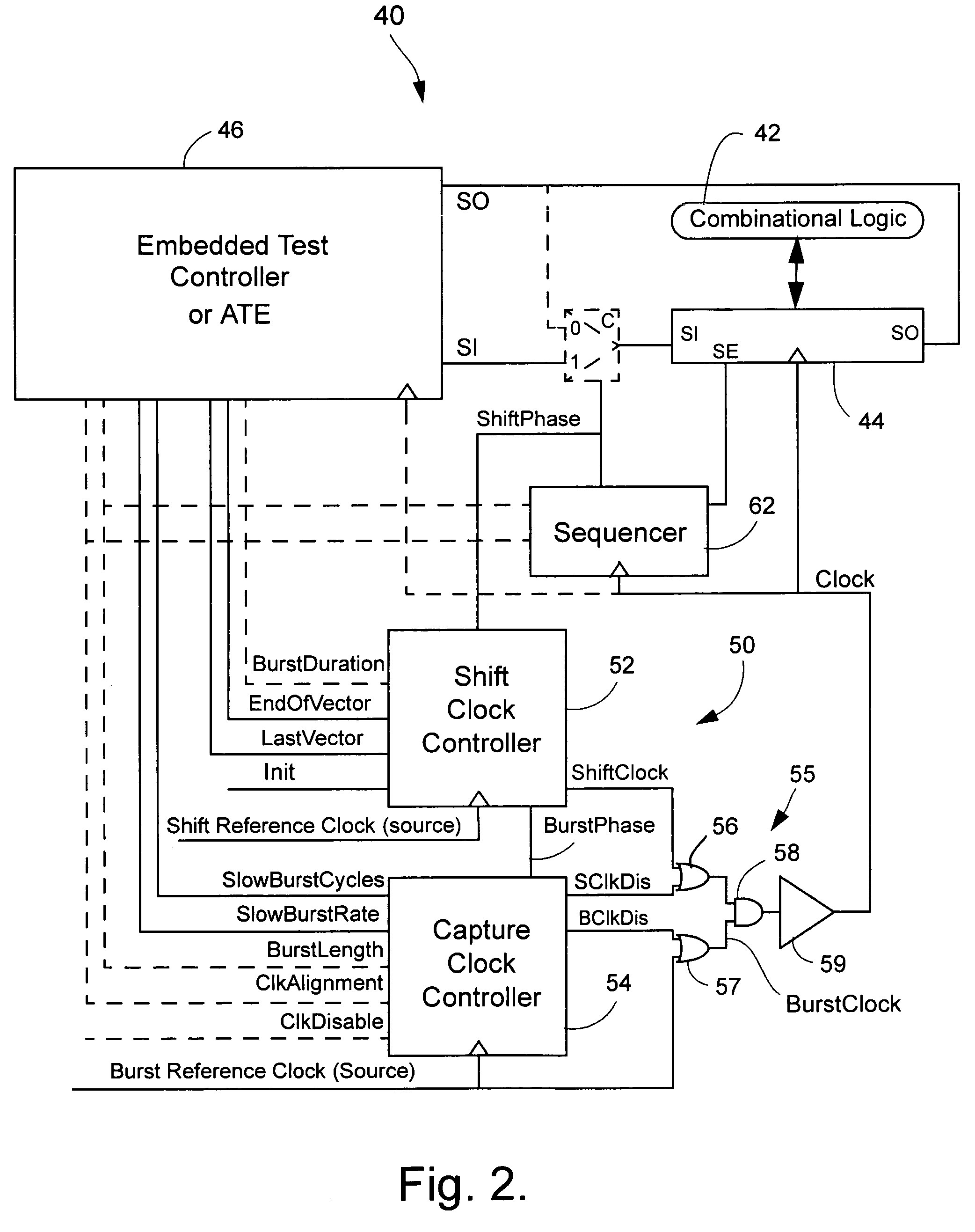
[0022]One aspect of the present invention provides a test clock controller to control, during a shift phase, the loading of test patterns and unloading of test response patterns into and from scan chains of an integrated circuit and to apply, during a burst phase, a burst of clock cycles derived from a reference clock in which the pattern is launched and the response of the circuit is captured. The test clock controller includes a shift clock controller which controls shift operations during the shift phase and one or more burst clock c...


PUM


Abstract

A test clock controller for generating a test clock signal for scan chains in integrated circuits having one or more clock domains, comprises a shift clock controller for generating a shift clock signal for use in loading test patterns into scan chains in the clock domains and for unloading a test response patterns from the scan chains and for generating a burst phase signal after loading a test pattern; and a burst clock controller associated with each of one or more clock domains and responsive to a burst phase signal for generating a burst of clock pulses derived from a respective reference clocks and including a first group of burst clock pulses having a selected reduced frequency relative to the reference clock and a second group of burst clock pulses having a frequency corresponding to that of the reference clock.

Description

CROSS-REFERENCE TO RELATED APPLICATIONS[0001]This application claims the benefit of U.S. Provisional Patent Application Ser. No. 60 / 564,210 filed Apr. 22, 2004, incorporated herein by reference.BACKGROUND OF THE INVENTION[0002]1. Field of the Invention[0003]The present invention generally relates to testing of integrated circuits and more, specifically, to a clock controller for use in at-speed testing of scan circuits.[0004]2. Description of Related Art[0005]Scan circuits are well known and generally consist of logic and scan chains comprised of memory elements which can be configured in a scan mode and a capture mode. The scan mode is used for shifting test patterns into the memory elements and for shifting the circuit response to the test patterns out of the memory elements. The capture mode is used to capture and store the response of the circuit in the memory elements.[0006]An at-speed test is typically performed by applying a short burst of two clock cycles to launch the test ...

Claims


Application Information

Patent Timeline
Patent Type & Authority Patents(United States)
IPC IPC(8): G01R31/28G01R31/3185G01R31/319
CPCG01R31/31858G01R31/31922G01R31/318552
Inventor NADEAU-DOSTIE, BENOITCOTE, JEAN-FRANCOIS
Owner SIEMENS PROD LIFECYCLE MANAGEMENT SOFTWARE INC
Why Eureka
Try Eureka