Universal calibration method for transmission path delay errors of parallel ADC sampling system

A technology of transmission path and delay error, which is applied in the field of alignment and calibration of multi-channel parallel data input delay in high-speed variable sampling system, can solve the problem that multiple sets of parallel ADC sampling systems are not universal, sampling system delay parameters are inconsistent, Difficulties in program version management and other issues, to achieve the effects of easy porting and version management, enhanced readability and standardization, and good application prospects

Active Publication Date: 2020-02-14
10TH RES INST OF CETC
View PDF7 Cites 23 Cited by
  • Summary
  • Abstract
  • Description
  • Claims
  • Application Information

AI Technical Summary

Problems solved by technology

The disadvantages of this method are: first, the delay parameter cannot adapt to the change of sampling frequency. When the sampling frequency changes, the delay parameter will change accordingly and needs to be recalibrated; A set of parallel ADC sampling systems is not universal. Due to the differences in the ADC chips themselves due to process reasons, each set of sampling systems needs to be calibrated separately; third, as the ambient temperature changes, the delay parameters of the ADC chip need to be fine-tuned; fourth, every The inconsistency of delay parameters in a sampling system leads to difficulties in program version management, especially for high-speed parallel ADC sampling systems with variable frequencies. The larger the frequency range, the more delay parameter files need to be saved, and the corresponding hardware program versions are also more complex. Lots of work

Method used


Image

  • Universal calibration method for transmission path delay errors of parallel ADC sampling system
  • Universal calibration method for transmission path delay errors of parallel ADC sampling system
  • Universal calibration method for transmission path delay errors of parallel ADC sampling system

Examples


Embodiment Construction

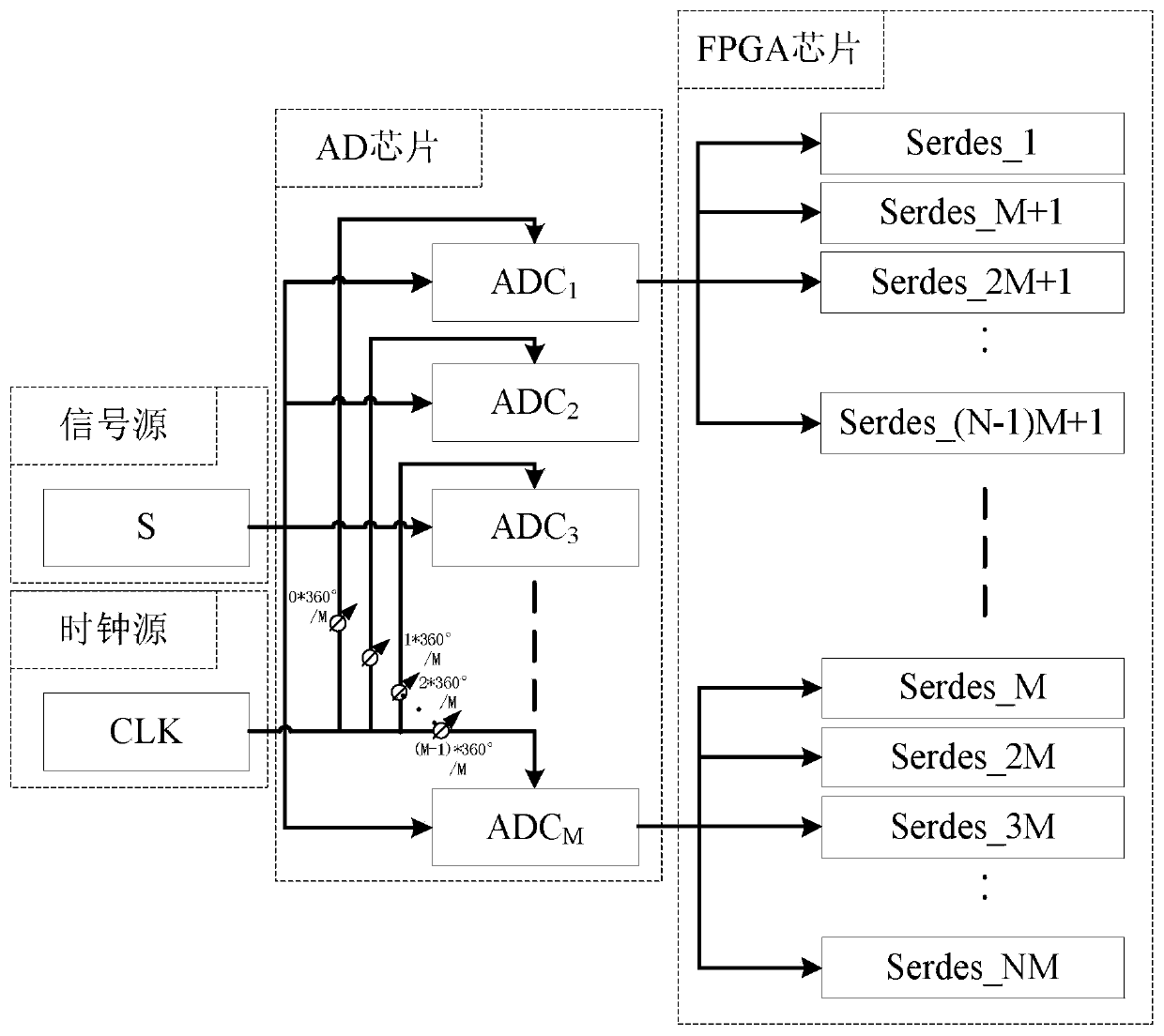
[0015] refer to figure 1. According to the present invention, the clock source CLK and the signal source S are configured as multi-channel output through an integrated M-channel high-speed analog-to-digital conversion AD chip, and the AD chip is connected to a large-scale programmable gate array FPGA through a high-speed serial interface to form a high-speed variable sampling rate system ; The AD chip transmits the high-speed sampling data grouped in parallel and reduces the speed through the parallel multi-channel mode to achieve the first level of speed reduction; by configuring the relevant registers, the parallel sampling data and the AD test sequence of each channel output phase relationship, FPGA adopts high-speed serial-to-parallel conversion The primitive ISERDES or the serial-to-parallel conversion IP core SelectIO converts high-speed serial data into parallel data to achieve the second level of speed reduction; the FPGA built-in program sets the virtual logic analyze...


PUM


Abstract

The invention provides a universal calibration method for transmission path delay errors of a parallel ADC sampling system, and aims to provide a universal method capable of adapting to sampling frequency changes and correcting multichannel data input delay. According to the technical scheme, a clock and a signal are configured into multi-channel output through an AD chip integrated with M channels, and an AD is connected with an FPGA through a serial peripheral interface to form a high-speed variable sampling rate system. The AD performs multi-channel parallel sampling on high-speed signals to realize first-stage speed reduction, and the FPGA performs serial-parallel conversion by adopting serial-parallel conversion primitives or serial-parallel conversion IP cores to realize second-stagespeed reduction. After the FPGA configures an AD to send a test sequence, a calibration instruction and a state machine are started, a time delay parameter calibration algorithm is operated, time delay parameters are dynamically placed into an FPGA input time delay control primitive, all data lines in channels and among the channels are aligned, the AD exits from the test sequence to output actual signals, and system input time delay calibration is completed.

Description

technical field [0001] The invention relates to an alignment calibration method for multi-channel parallel data input delay of a high-speed variable sampling system composed of an ADC device with a high-speed parallel interface and an FPGA. [0002] technical background [0003] At present, modern electronic signals are characterized by complexity and diversity, especially the rapid growth of broadband and non-stationary characteristics. seam testing requirements. High-precision sampling has become the bottleneck of modern time-domain test instruments. The higher the sampling rate and sampling accuracy, the stronger the ability to restore the signal. In recent years, the ADC sampling rate has been greatly improved, but it is still difficult to balance high speed and high precision. This is limited by the current analog device manufacturing process. of. With the promotion of digital technology, higher and higher requirements are put forward for the sampling rate and samplin...

Claims


Application Information

Patent Timeline
Patent Type & Authority Applications(China)
IPC IPC(8): H03M1/10H03M1/12
CPCH03M1/1014H03M1/123H03M1/1245
Inventor 胡洪马力科张晓波唐洪军吴江
Owner 10TH RES INST OF CETC
Why Eureka
Try Eureka