Techniques for manufacturing a circuit board having a countersunk via

a technology of countersunk vias and circuit boards, which is applied in the manufacture of printed circuits, printed circuits, printed circuit aspects, etc., can solve the problems of significant increase in costs, difficulty for circuit board manufacturers to achieve connectivity goals using through vias alone, and thicker and more massive circuit boards. achieve the effect of reducing costs, improving access, and high connection density

Active Publication Date: 2007-01-02
EMC IP HLDG CO LLC
View PDF24 Cites 38 Cited by
  • Summary
  • Abstract
  • Description
  • Claims
  • Application Information

AI Technical Summary

Benefits of technology

[0010]In contrast to the above-described conventional vias, embodiments of the invention are directed to circuit board manufacturing techniques which involve carving a countersunk via hole within circuit board material to form a countersunk via. Such carving is capable of taking place at the same time as the drilling process for creating through vias thus alleviating the need for an additional expensive laminating and pressing process (e.g., as when creating conventional blind and buried vias). Additionally, the countersunk via resulting from such carving is capable of interconnecting several internal signal layers thus providing greater opportunity to achieve high connection densities and thus perhaps alleviating the need for additional circuit board layers to reduce costs even further.
[0011]One embodiment of the invention is directed to a method for manufacturing a circuit board. The method includes obtaining a plane-shaped structure having layers of circuit board material integrated together, and carving a hole within the plane-shaped structure (e.g., using a single countersinking drill bit). The carved hole includes an inner portion having a substantially uniform inner portion diameter and a connecting portion disposed between the inner portion and an outer surface of the plane-shaped structure. At least part of the connecting portion has a diameter which is larger than the substantially uniform inner portion diameter of the inner portion to improve access to the inner portion. The method further includes performing a plating process on the plane-shaped structure to provide plating over the hole carved within the plane-shaped structure. The provided plating forms a countersunk via which provides an electrical pathway from the outer surface of the plane-shaped structure to an internal circuit board trace.

Problems solved by technology

Unfortunately, there are deficiencies to circuit boards which use only the above-described conventional through, blind and buried vias.
For example, in connection with the above-described conventional through vias, it is difficult for circuit board manufacturers to achieve connectivity goals using through vias alone.
Nevertheless, one way to continue to use through vias exclusively is for circuit board manufacturers to add circuit board layers resulting in thicker and more massive circuit boards which significantly raises costs.
However, at some point, such features are no longer manufacturable in a reliable manner even though special processes are available such as pulse plating and plasma hole wall preparation (e.g., the smaller the via diameter the greater the narrow chimney effect on the via being plated and cleaned).
Additionally, in connection with conventional blind vias, creation of blind vias can be expensive and the use of blind vias can be limited.
In particular, when creating blind vias by combining multiple circuit board sections having through vias, the lamination and pressing process provides a substantial increase in manufacturing costs due to the need for additional equipment such as tooling and handling equipment needed to align circuit board sections, X-ray registration equipment, etc.
Even with such equipment, there is never 100% yield (e.g., due to registration errors) and, as a result, there is opportunity to lose significant added value during the lamination and pressing process.
Furthermore, when creating conventional blind vias by drilling partially into circuit boards, design rule constraints limit the depth and width of the blind vias available to the circuit board manufacturer.
That is, if the manufacturer attempts to create blind via holes which go beyond the design rule aspect ratio by making the blind vias too deep, the manufacturer will be unable to properly clean and plate the blind vias.
Without the ability to set blind vias more deeply into the circuit boards, circuit board manufactures are unable to truly utilize blind vias due to routing channel restrictions (i.e., not enough space within the circuit board to connect traces to the blind vias).
Moreover, with conventional blind vias and dog bone configurations, there is typically very little space left to properly form electrically tuned anti-pads for proper impedance control.
Moreover, in connection with conventional buried vias, creation of buried vias within circuit boards is very expensive.
In particular, creating buried vias requires a lamination and pressing process thus providing a substantial increase in manufacturing costs due to the need for additional equipment.
Additionally, as mentioned above in connection with buried vias, there is never 100% yield and, as a result, there is increased opportunity to lose a significant amount of added value by less than perfect yields in the additional lamination and pressing processing.

Method used


Image

  • Techniques for manufacturing a circuit board having a countersunk via
  • Techniques for manufacturing a circuit board having a countersunk via
  • Techniques for manufacturing a circuit board having a countersunk via

Examples


Embodiment Construction

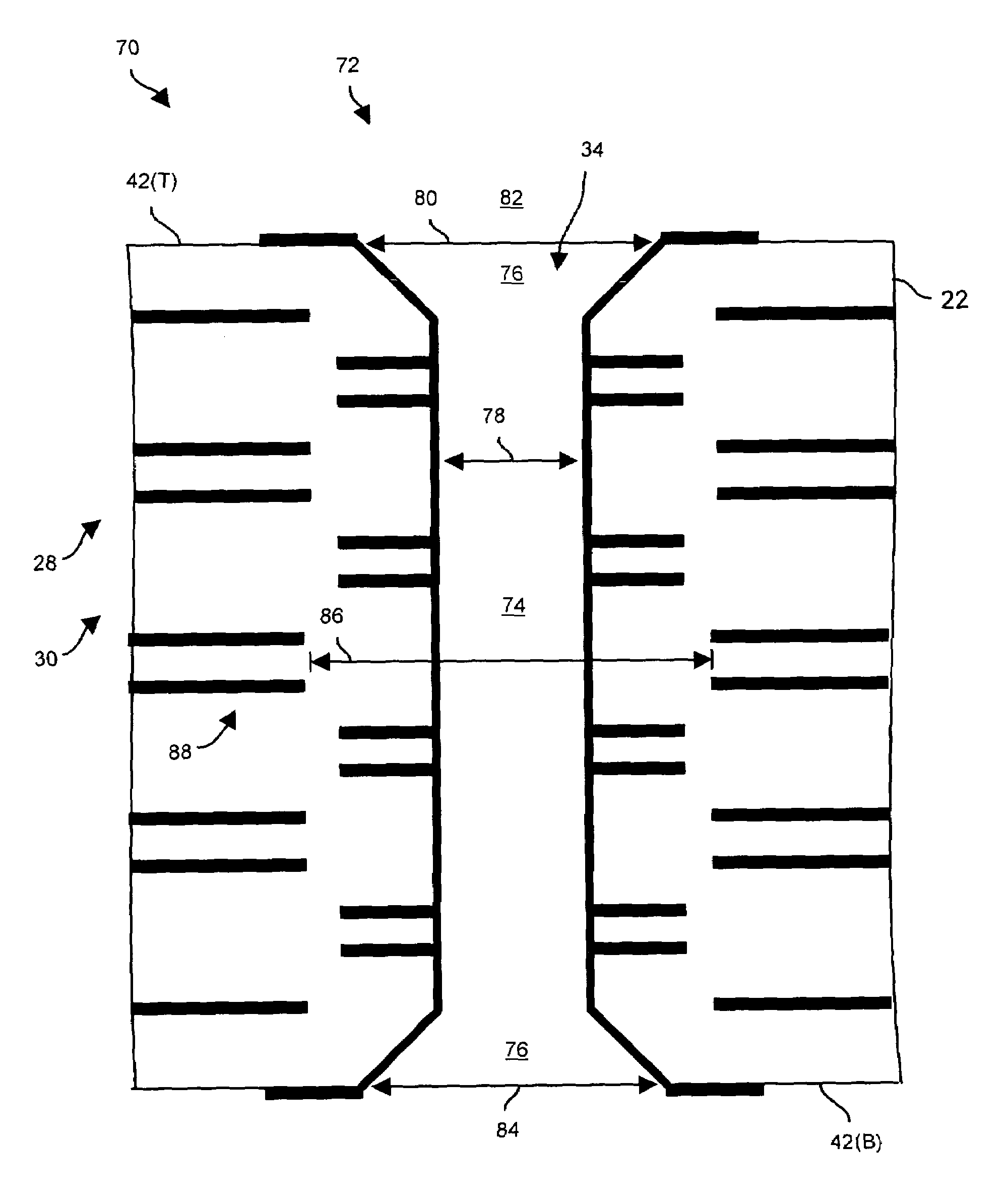
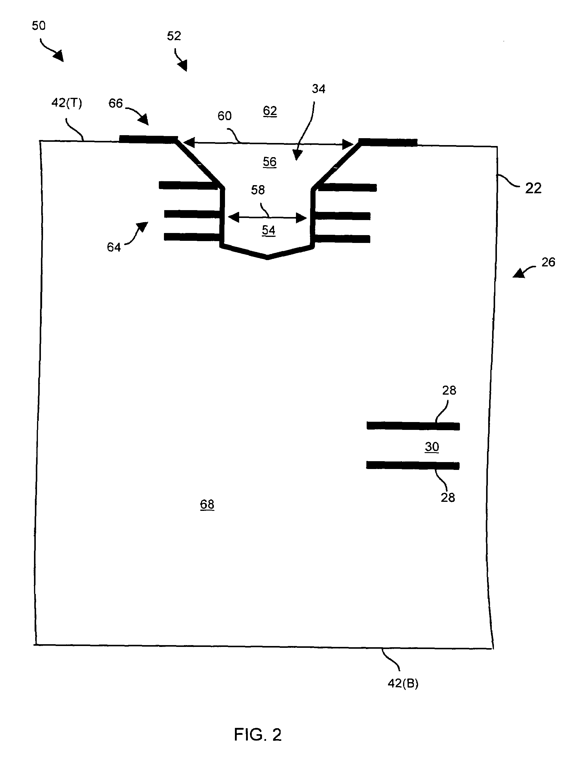
[0024]Embodiments of the invention are directed to circuit board manufacturing techniques which involve carving a countersunk via hole within circuit board material to form a countersunk via. Such carving is capable of taking place at the same time as the drilling process for creating through vias thus alleviating the need for an additional laminating and pressing process which would otherwise increase costs (e.g., as required when creating conventional blind and buried vias). Furthermore, the countersunk via resulting from such carving is capable of interconnecting several internal signal layers by going deeper into the circuit board material than a conventional blind via without posing a manufacturability or quality threat thus providing greater opportunity to achieve high connection densities and thus perhaps alleviating the need for one or more additional circuit board layers.

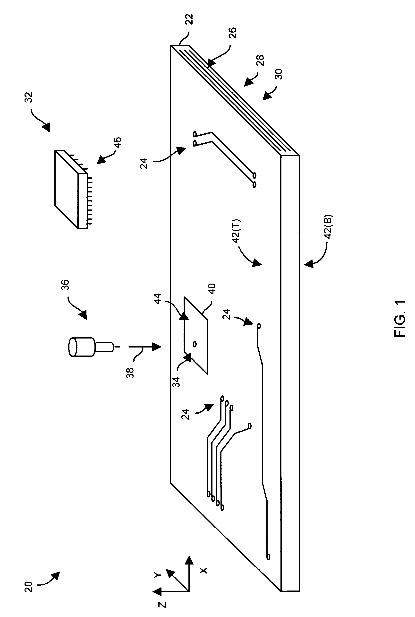
[0025]FIG. 1 shows a fabricated circuit board 20 which is suitable for use by the invention. The fabrica...


PUM

PropertyMeasurementUnit
diameteraaaaaaaaaa
diameteraaaaaaaaaa
diameteraaaaaaaaaa

Abstract

A technique for manufacturing a circuit board involves obtaining a plane-shaped structure having layers of circuit board material integrated together, and carving a hole within the plane-shaped structure (e.g., using a single countersinking drill bit). The carved hole includes an inner portion having a substantially uniform inner portion diameter and a connecting portion disposed between the inner portion and an outer surface of the plane-shaped structure. At least part of the connecting portion has a diameter which is larger than the substantially uniform inner portion diameter of the inner portion to improve access to the inner portion. The technique further involves
    • performing a plating process on the plane-shaped structure to provide plating over the hole carved within the plane-shaped structure. The provided plating forms a countersunk via which provides an electrical pathway from the outer surface of the plane-shaped structure to an internal circuit board trace.

Description

BACKGROUND OF THE INVENTION[0001]In general, a via is a hole within a circuit board which is lined with conductive material (e.g., copper, nickel, etc.) to provide an electrical pathway between multiple conductive layers of the circuit board. A typical circuit board includes many vias in order to achieve layer-to-layer interconnections between various conductive circuit board features (e.g., surface pads and traces, inner functional signal layers, power planes, ground planes, etc.).[0002]One type of via, which extends completely through a circuit board (i.e., from one outer surface to the other outer surface on the opposite side of the circuit board), is called a “through via”. Some circuit board manufacturers do not draw distinctions between the term “through via” and the term “plated through hole” (PTH), which refers to a structure that is intended to support a component lead (e.g., a pin in hole configuration). Accordingly, within this document, the term “through via” is intended...

Claims


Application Information

Patent Timeline
Patent Type & Authority Patents(United States)
IPC IPC(8): H01K3/10
CPCH05K1/112H05K3/0047H05K3/429H05K1/115Y10T29/49165H05K3/3421H05K3/3478H05K3/421H05K2201/09472H05K2201/09518H05K2201/09827H05K2201/09845H05K2203/0207H05K2203/041Y10T29/49117Y10T29/49147Y10T29/49149
Inventor DOWNES, STUART D.FEINSTEIN, LOUIS H.
Owner EMC IP HLDG CO LLC
Why Eureka
Try Eureka