PLL modulation circuit and polar modulation apparatus

a modulation circuit and polar modulation technology, applied in modulation, pulse technique, digital transmission, etc., can solve the problems of deterioration in modulation accuracy, deterioration in noise characteristics, etc., and achieve the effect of improving modulation accuracy

Inactive Publication Date: 2007-01-02
PANASONIC CORP
View PDF3 Cites 23 Cited by
  • Summary
  • Abstract
  • Description
  • Claims
  • Application Information

AI Technical Summary

Benefits of technology

[0017]It is therefore an object of the present invention to provide a PLL modulation circuit and polar modulation apparatus that improves modulation accuracy.

Problems solved by technology

However, widening the bandwidth of the PLL modulation circuit has the risk of causing deterioration in noise characteristics.
When a modulation signal cannot maintain flat characteristics, this might cause deterioration in modulation accuracy.
This is a factor that causes deterioration in modulation accuracy.
Thus, preparing modulation sensitivity table 7 requires a great amount of time and might even increase manufacturing costs.
If then there is a time gap between the modulation signals, this lowers the modulation accuracy.
The above description of a conventional PLL modulation circuit does not explain the method of adjusting the time gap between two points, and the setting of adequate timings poses difficulty.
However, as described above, the conventional PLL modulation circuit suffers decrease in the modulation level and time gap between two points and thus has difficulty improving the modulation accuracy.

Method used


Image

  • PLL modulation circuit and polar modulation apparatus
  • PLL modulation circuit and polar modulation apparatus
  • PLL modulation circuit and polar modulation apparatus

Examples


embodiment 1

(Embodiment 1)

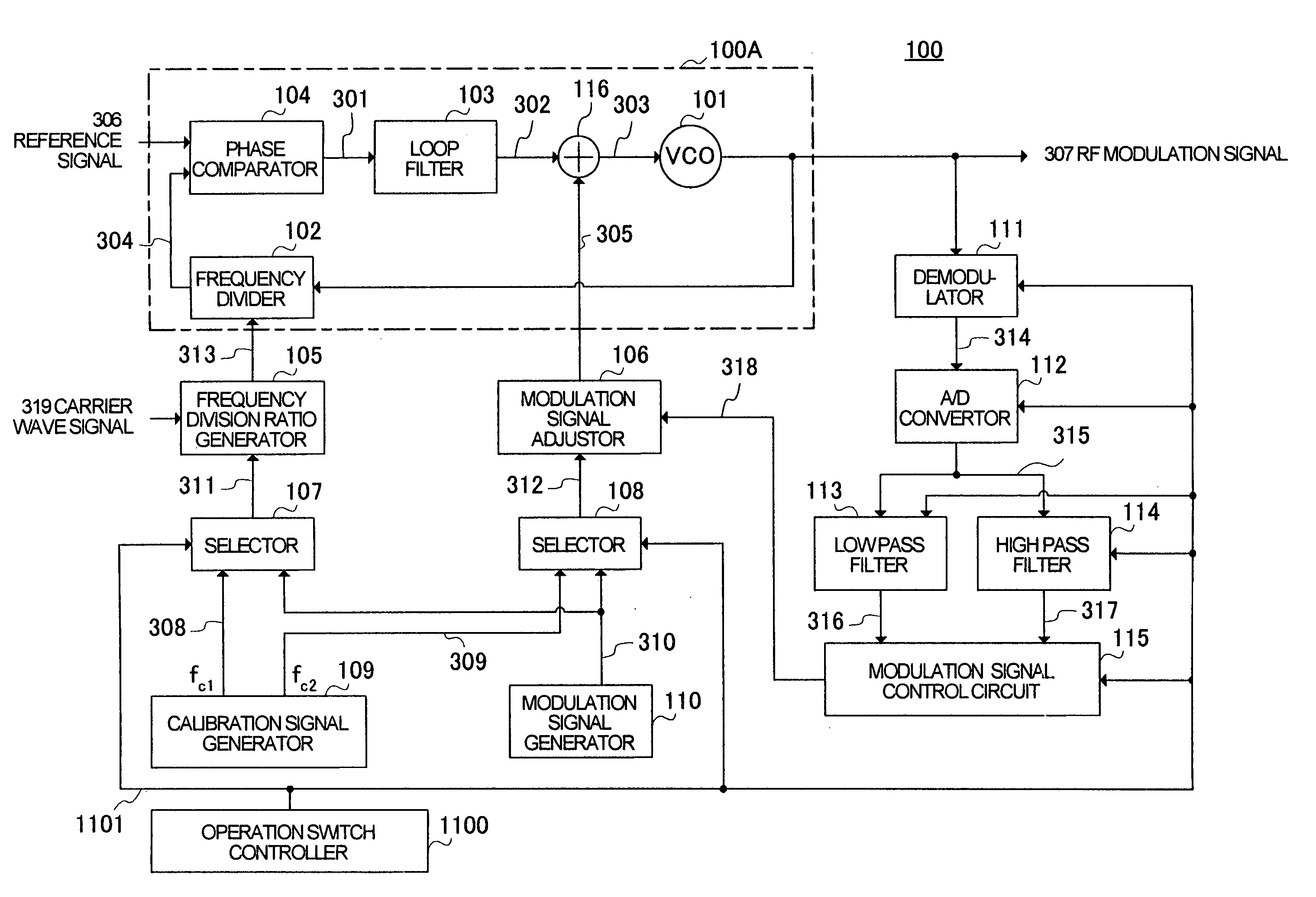
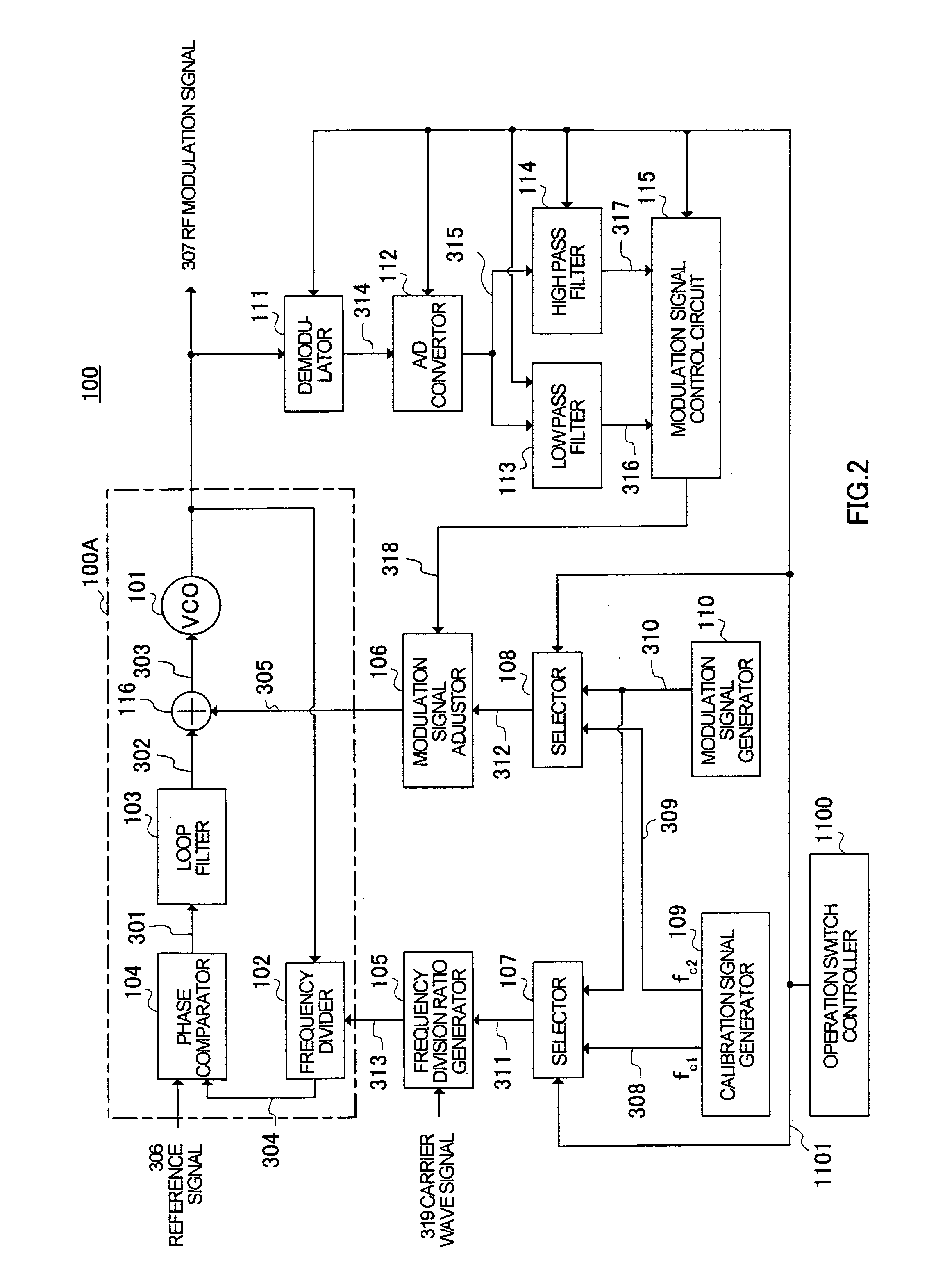
[0034]FIG. 2 shows a simplified configuration of a PLL modulation circuit according to Embodiment 1 of the present invention. As shown in FIG. 2, PLL modulation circuit 100 according to Embodiment 1 of the present invention has PLL section 100A, which includes voltage controlled oscillator (VCO) 101, frequency divider 102, phase comparator 104, loop filter 103 and adder 116. VCO 101 changes the oscillation frequency in accordance with the voltage inputted in the control voltage terminal. Frequency divider 102 divides the frequency of RF modulation signal 307 outputted from VCO 101. Phase comparator 104 compares the phase of output signal 304 of frequency divider 102 and the phase of reference signal 306 and outputs a signal in accordance with the phase difference between the two signals. Loop filter 103 outputs signal 302, which is an equalized version of output signal 301 of phase comparator 104. Adder 116 adds the value of signal 302 from loop filter 103 and the valu...

embodiment 2

(Embodiment 2)

[0054]FIG. 11 is a block diagram showing the configuration of a polar modulation apparatus according to Embodiment 2 of the present invention. Parts in Embodiment 2 of the present invention that are identical to ones in Embodiment 1 will be assigned the same reference numerals as in Embodiment 1 without further explanations.

[0055]As shown in FIG. 11, polar modulation apparatus 200 according to Embodiment 2 of the present invention has PLL modulation circuit 100 of Embodiment 1 of the present invention, and, in addition, non-linear power amplifier201 and amplitude modulation signal generator 202.

[0056]RF modulation signal 307 from VCO 101 of PLL modulation circuit 100 is inputted in non-linear power amplifier 201 as a phase modulation signal. Amplitude modulation signal generator 202 generates amplitude modulation signal 2021 ad sends it to non-linear power amplifier 201 as a control signal. In accordance with the voltage value of amplitude modulation signal 2021, non-l...

embodiment 3

(Embodiment 3)

[0059]FIG. 12 is a block diagram showing the configuration of a wireless communication apparatus according to Embodiment 3 of the present invention. Parts in Embodiment 3 of the present invention that are identical to ones in Embodiment 2 will be assigned the same reference numerals without further explanations.

[0060]As shown in FIG. 12, wireless communication apparatus 400 according to Embodiment 3 of the present invention has PLL modulation circuit 100, non-linear power amplifier 201, and amplitude modulation signal generator 202 in polar modulation apparatus 200 of Embodiment 2 of the present invention, and, in addition, transmission and reception switch 401, antenna 402, and receiver 403. Transmission and reception switch 401 switches between supplying transmission signals from PLL modulation circuit 100 of polar modulation apparatus to antenna 402 and supplying received signals from antenna 402 to receiver 403. Non-linear power amplifier 201 sends output transmiss...


PUM


Abstract

First and second calibration signals (308, 309) are sent to a frequency divider (102) and an adder (116) of a PLL section (100A), demodulated in a demodulator (111), filtered through a low pass filter (113) and a high pass filter (114) and thereafter sent to a modulation signal control circuit (115). The modulation signal control circuit (115) generates control information (318) in comparison with the phase and amplitude of the first and second calibration signals (308 and 309) and sends the control information (318) to a modulation control signal generator (106). Modulation control signal generator (106) holds the control information (318) and controls the values of the first modulation signal and second modulation signal sent to the frequency divider (102) and adder (116) on the based on the control information (318) held in modulation operation.

Description

BACKGROUND OF THE INVENTION[0001]1. Field of the Invention[0002]The present invention relates to PLL modulation circuit and polar modulation apparatus in wireless communication apparatus.[0003]2. Description of the Related Art[0004]Generally speaking, the PLL (Phase Locked Loop) modulation circuit is expected to realize low costs, low power consumption, and excellent noise characteristics and modulation accuracy. To improve the modulation accuracy of a PLL modulation circuit, the PLL frequency bandwidth (i.e. PLL bandwidth) is preferably wider than the frequency bandwidth of the modulation signal (i.e. modulation bandwidth).[0005]However, widening the bandwidth of the PLL modulation circuit has the risk of causing deterioration in noise characteristics. So, as a technique for enabling a wideband PLL modulation circuit, two-point modulation is presently proposed whereby the bandwidth of a PLL modulation circuit is set narrower than the bandwidth of a modulation signal and modulation ...

Claims


Application Information

Patent Timeline
Patent Type & Authority Patents(United States)
IPC IPC(8): H03C3/00H03C5/00H03L7/00
CPCH03C5/00H03C3/0916H03C3/095H03C3/0991
Inventor MITANI, YOSUKEHIRANO, SHUNSUKE
Owner PANASONIC CORP
Why Eureka
Try Eureka