

Semiconductor memory device with MOS transistors, each including a floating gate and a control gate, a control method thereof, and a memory card including the same
a technology of semiconductor memory and transistors, applied in transistors, solid-state devices, instruments, etc., can solve the problems of difficult miniaturization of lsi and large size of write circuits
- Summary
- Abstract
- Description
- Claims
- Application Information
AI Technical Summary
Benefits of technology
Problems solved by technology
Method used
Image

Examples
first embodiment
[0125]As described above, the flash memory produces the following effects.
[0126](1) The flash memory can be made smaller
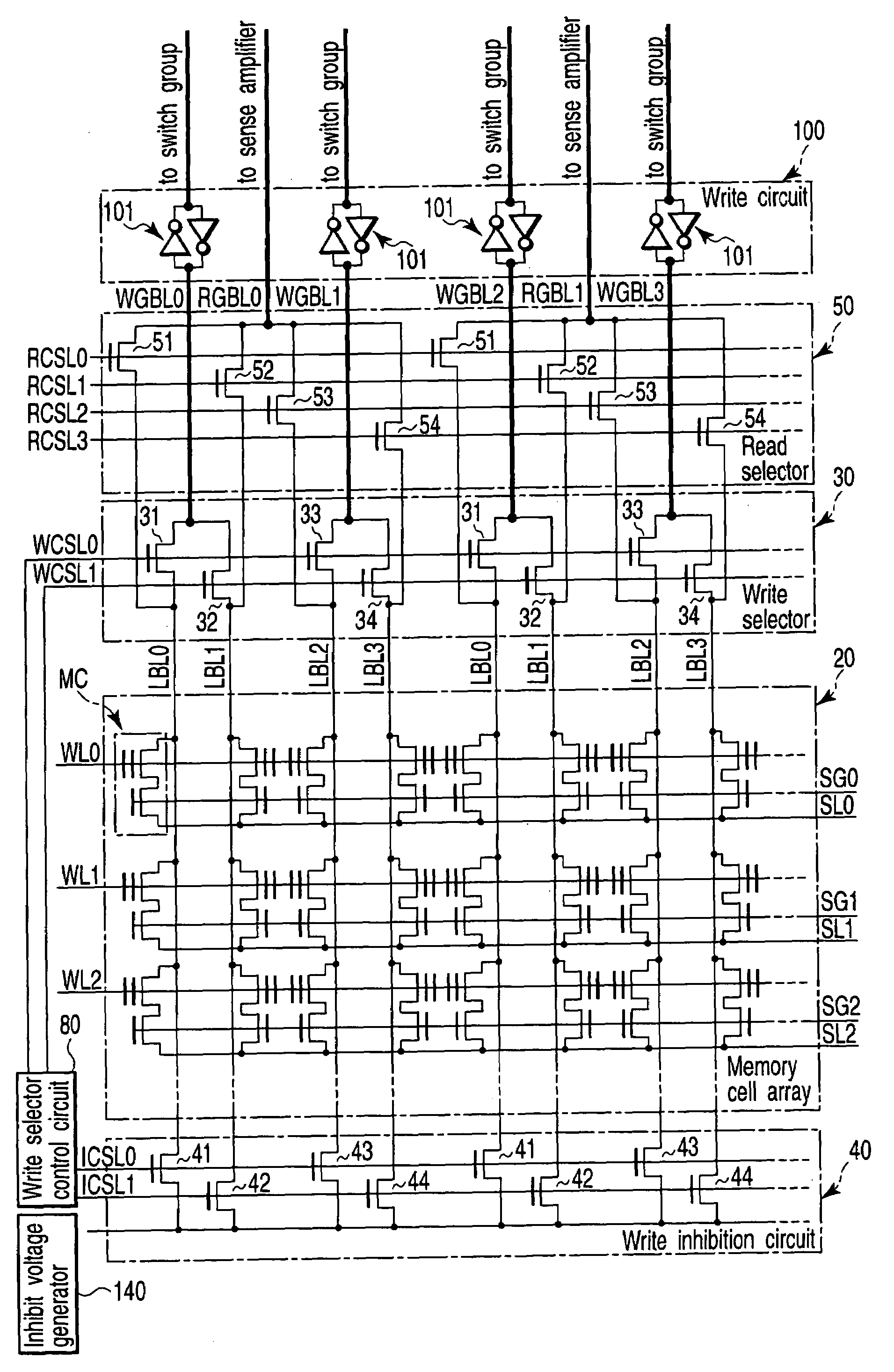
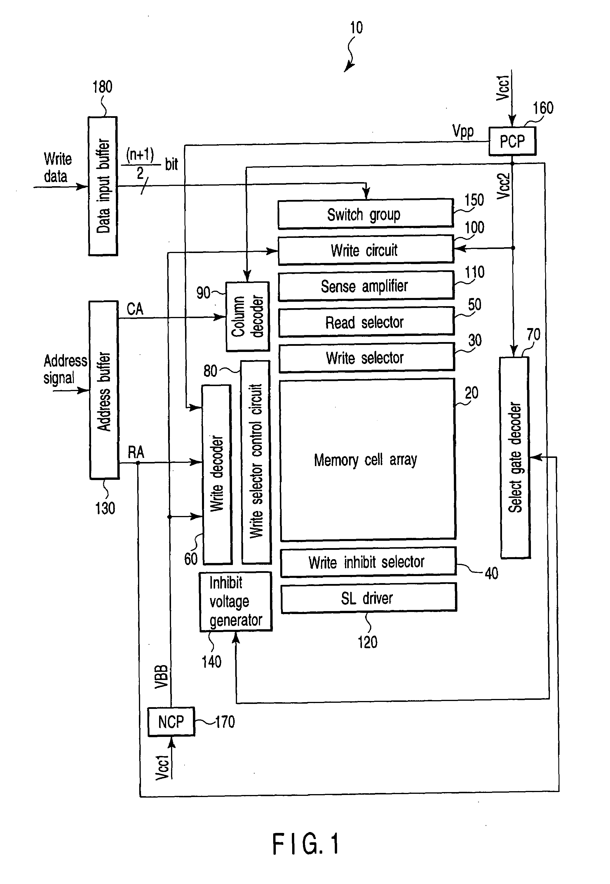
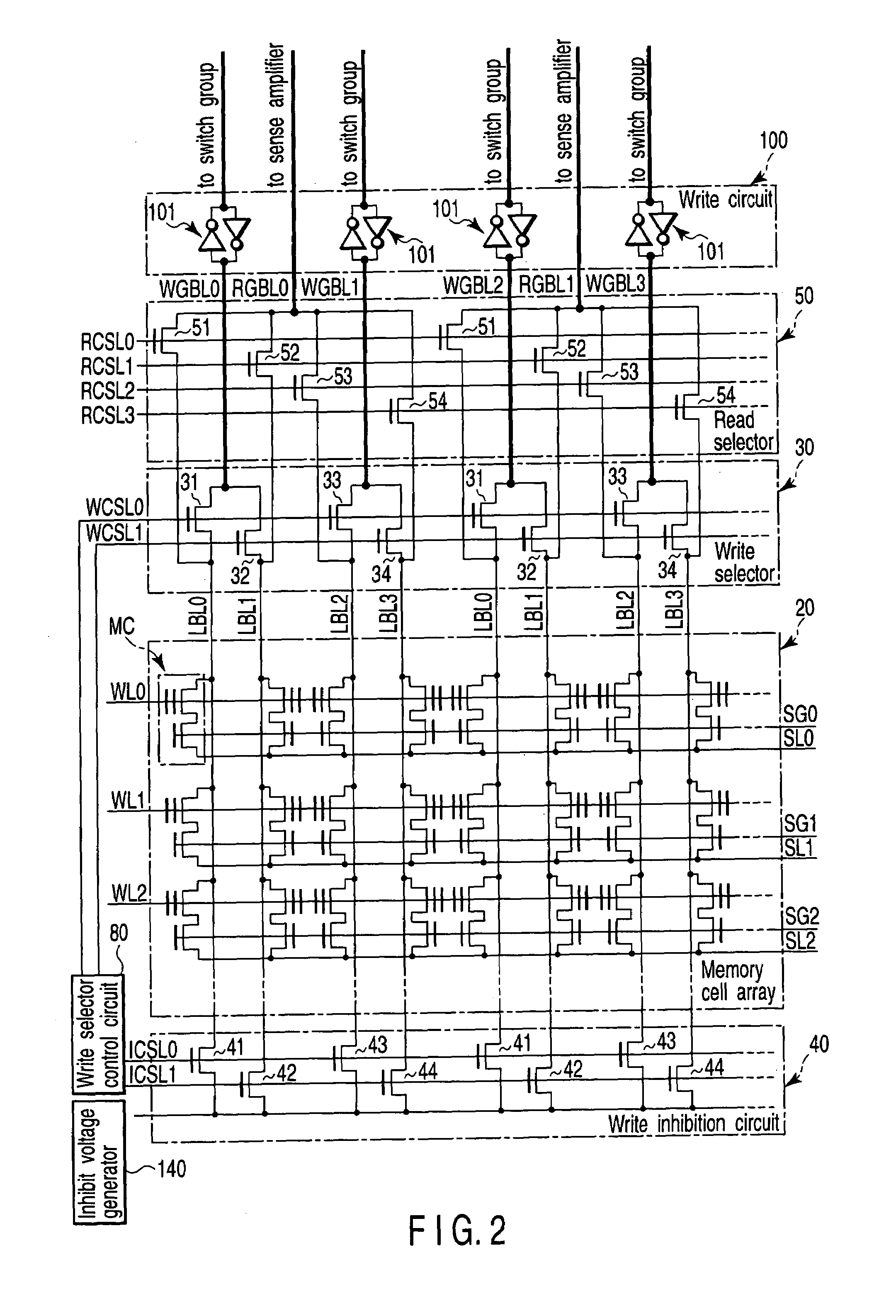
[0127]With configuration of the first embodiment, the switch group 150 which transfers the input data from the data input buffer 180 to the write circuit 100 includes only n-channel MOS transistors 151. Therefore, the size of the switch group can be made smaller than when the switch group includes p-channel MOS transistors or when it includes a combination of n-channel MOS transistors and p-channel MOS transistors. Consequently, the flash memory can be made smaller.
[0128](2) The read operation reliability can be improved
[0129]With the configuration of the first embodiment, in a read operation, the reset transistor 106 causes the potentials on the write global bit lines to go to 0V. This reduces noise on the read global bit lines caused by the write global bit lines, when the write global bit lines are close to the read global bit lines. As a result, the read opera...
second embodiment
[0138]Next, a data latch operation in the flash memory of the second embodiment will be explained using FIGS. 15 and 16. FIG. 15 is a flowchart for a data latch operation. FIG. 16 is a circuit diagram to help explain the write circuit 100 and write inhibit control circuit 190 in a data latch operation.
[0139]First, after step S20 to step S22 explained in FIG. 7, write data is input (step S40). Here, as shown in FIG. 16, it is assumed that the number of write global bit lines is 512. If the externally input data are for 512 lines, that is, if the externally input data contain 512 bits (step S41), the latch circuits 101 latch the data allocated to the respective latch circuits by the processes in step S24 to step S27. On the other hand, if the externally input data contains less than 512 bits (step S41), the write inhibit control circuit 190 inputs “1” data to the latch circuits 101 to which no data is input (step S42). The process in step S42 will be explained using FIG. 16.
[0140]As s...
third embodiment
[0177]The LSI of the third embodiment produces not only the effects in items (1) to (4) but also the following effect in item (5).
[0178](5) It is possible to mount a plurality of types of flash memories on a single chip, while suppressing the manufacturing cost.
[0179]The memory cell transistors MT and select transistors ST1, ST2, ST included in the NAND flash memory 500, 3Tr-NAND flash memory 600, and 2Tr flash memory 10 are formed in the same processes. That is, the individual MOS transistors are formed in the same oxidizing process, film-forming process, impurity implanting process, and photolithographic etching process. As a result, the gate insulating film 240, inter-gate insulating film 260, the floating gates 250 and control gates 270 of the memory cell transistors MT, and the select gates 250, 270 of the select transistors are the same in the three flash memories 10, 500, 600. In such a manufacturing method, the memory cell arrays of the three flash memories can be formed by ...
PUM
 Abstract
Description
Claims
Application Information