Semiconductor device and a method of manufacturing the same

a technology of semiconductor devices and semiconductors, applied in semiconductor devices, semiconductor/solid-state device details, electrical devices, etc., can solve the problem of not negligible external resistance, and achieve the effect of reducing thermal resistance and packaging heigh

Inactive Publication Date: 2007-01-09
RENESAS ELECTRONICS CORP
View PDF13 Cites 7 Cited by
  • Summary
  • Abstract
  • Description
  • Claims
  • Application Information

AI Technical Summary

Benefits of technology

[0023]As a result, since an inner lead coupling portion for supporting each of the inner leads is directly connected to the semiconductor pellet by the respective connecting portion, external resistance can be lower than that in the case of electrical connection using bonding wires.
[0024]Since the outer leads formed in a gull wing configuration and the header mechanically and electrically connected to the semiconductor pellet can be surface-mounted on a printed circuit board, a further reduction of external resistance can be achieved.
[0025]Since the header is separate from the inner leads, the radiating performance of the header can be improved by forming it using a material having preferable radiating performance irrespectively of the material of the inner leads. Further, since the header is surface-mounted on a printed circuit board, heat from the semiconductor pellet can be effectively released to the printed circuit board as a result of thermal conduction, which makes it possible to improve the radiating performance further.
[0035]This makes it possible to reduce the thermal resistance of the semiconductor device further.

Problems solved by technology

However, when the magnitude of the external resistance exceeds about 50% of the entire resistance as a result of technical advances toward improvements to reduce the internal resistance, situations occur wherein the external resistance is not negligible.

Method used


Image

  • Semiconductor device and a method of manufacturing the same
  • Semiconductor device and a method of manufacturing the same
  • Semiconductor device and a method of manufacturing the same

Examples


Embodiment Construction

[0087]The following description of preferred embodiments will not refer to identical or similar parts repeatedly unless necessity arises.

[0088]While a preferred embodiment will be described as a plurality of sections or a plurality of embodiments where it is necessary for convenience, they are related to each other instead of being independent, e.g., one embodiment may be a partial or overall modification of another embodiment or may be detailed or supplementary description of another embodiment unless otherwise specified.

[0089]When the number of elements and the like (number of elements, numerical values, quantities, ranges and the like) are mentioned in the context of the following embodiment, the particularly mentioned quantities will not limit the invention, and quantities above or below the particular quantities may be used instead unless otherwise specified or unless the particular quantities are limiting in view of the principle of the invention.

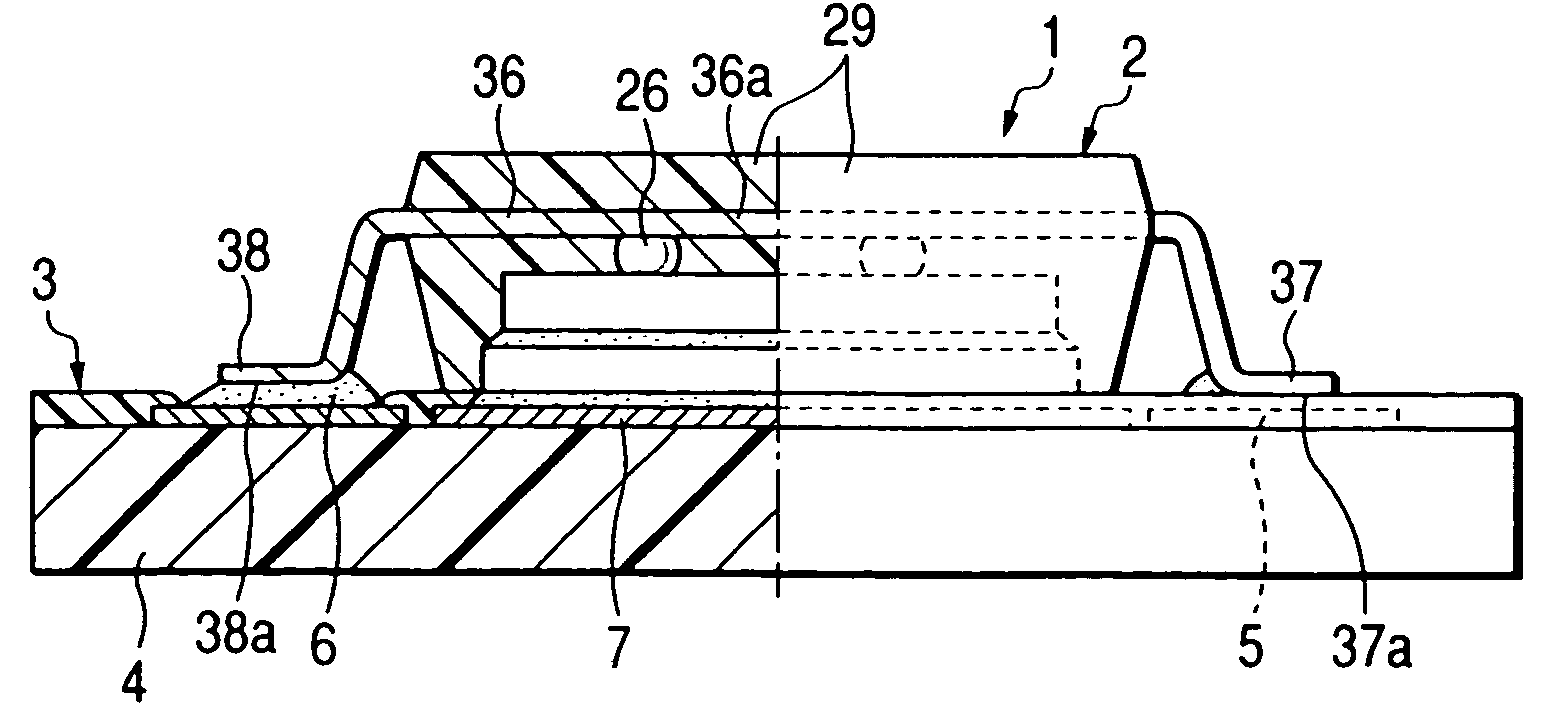
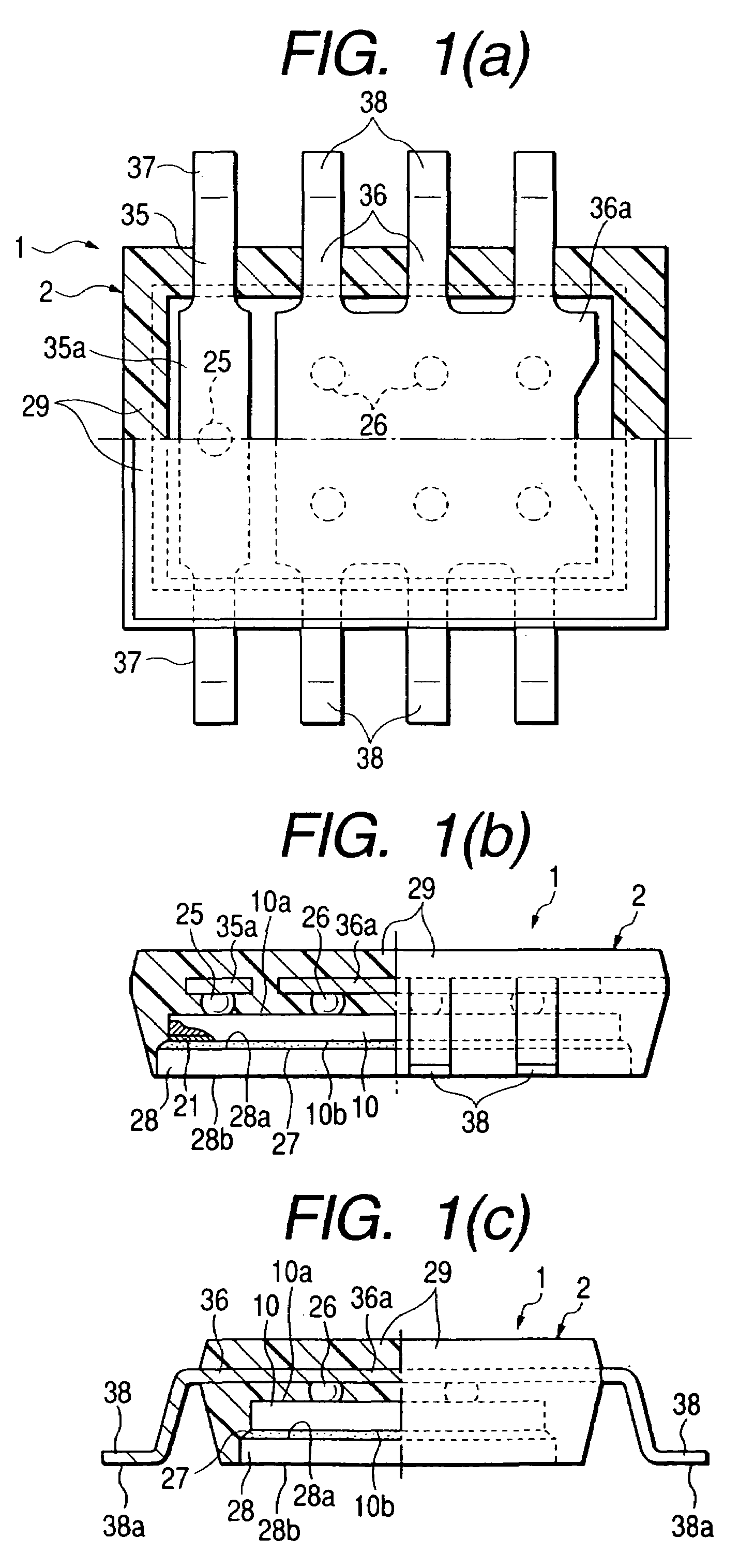
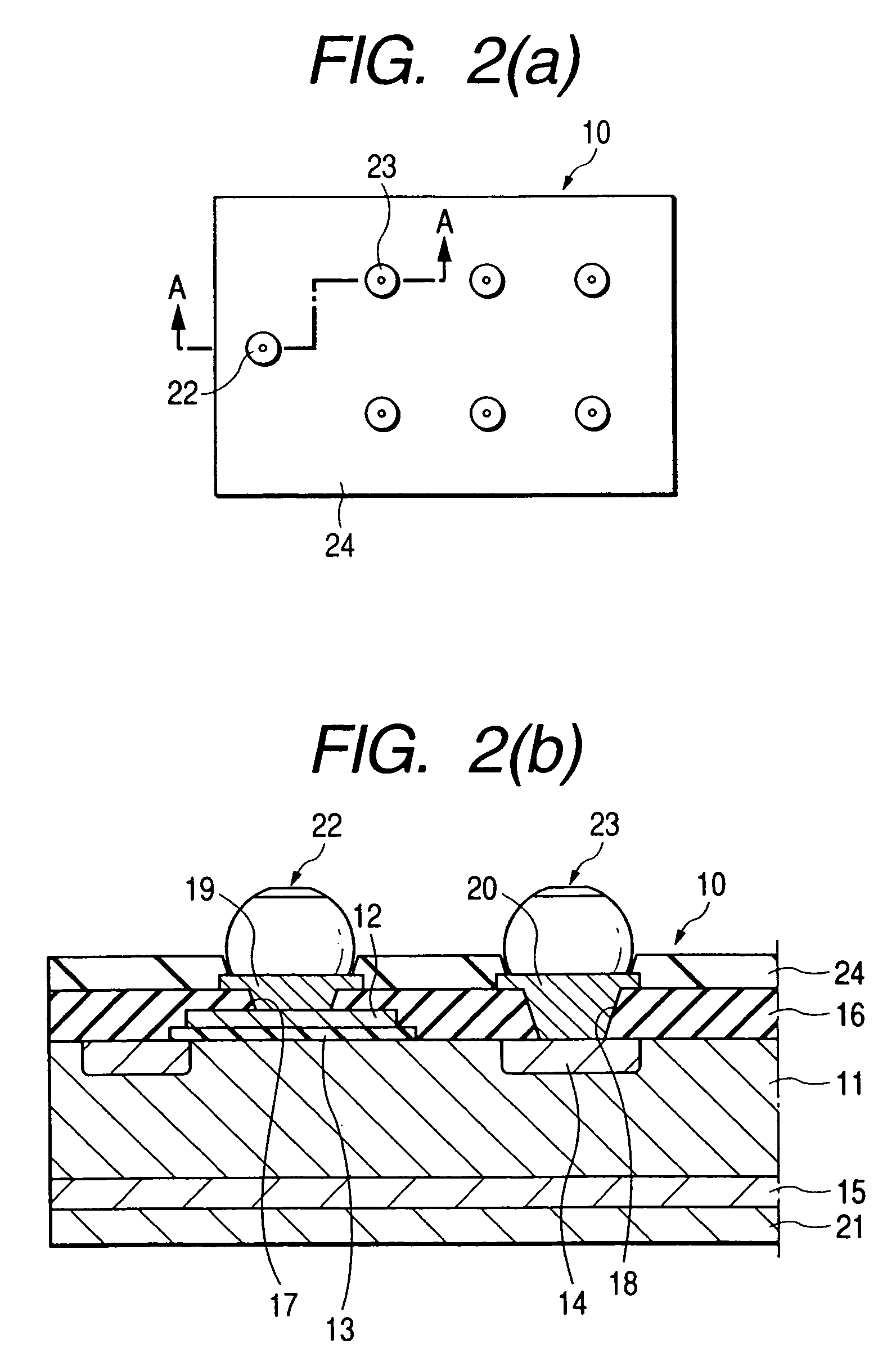
[0090]A preferred embodiment o...


PUM


Abstract

A semiconductor device and method having high output and having reduced external resistance is reduced and improved radiating performance. A MOSFET (70) has a connecting portion for electrically connecting a surface electrode of a semiconductor pellet and a plurality of inner leads, a resin encapsulant (29), a plurality of outer leads (37), (38) protruding in parallel from the same lateral surface of the resin encapsulant (29) and a header (28) bonded to a back surface of the semiconductor pellet and having a header protruding portion (28c) protruding from a lateral surface of the resin encapsulant (29) opposite to the lateral surface from which the outer leads protrude, wherein the header (28) has an exposed surface (28b) exposed from the resin encapsulant (29); the outer leads (37), (38) are bent; and the exposed of the outer leads (37), (38) are provided at substantially the same height.

Description

[0001]This is a continuation application of U.S. Ser. No. 10 / 265,324, filed Oct. 7, 2002 (now U.S. Pat. No. 6,812,554), which is a divisional application of U.S. Ser. No. 09 / 502,826, filed Feb. 11, 2000 (now U.S. Pat. No. 6,479,888).BACKGROUND OF THE INVENTION[0002]1. Field of the Invention[0003]The present invention relates to a semiconductor manufacturing technique and, more particularly, to a technique which is advantageously applied to high output MOSFETs (metal oxide semiconductor field effect transistors).[0004]2. Description of the Prior Art[0005]According to a study made by the inventor, exemplary semiconductor devices that generate high output and high heat include transistors referred to as “MOSFETs” which are used in electronic and electric apparatuses in all fields including power supplies and switches of battery-driven apparatuses, car electronics and controllers for driving motors.[0006]An example of such MOSFETs that generate high output and high heat is disclosed in ...

Claims


Application Information

Patent Timeline
Patent Type & Authority Patents(United States)
IPC IPC(8): H01L21/00H01L23/02H01L21/56H01L23/495H01L23/50
CPCH01L21/561H01L21/565H01L23/4951H01L23/49562H01L24/81H01L2924/1305H01L2924/1306H01L2224/32245H01L2224/16245H01L2224/81801H01L2924/01004H01L2924/01013H01L2924/01029H01L2924/01078H01L2924/01079H01L2924/01082H01L2924/01322H01L2924/13055H01L2924/13091H01L2924/01005H01L2924/01006H01L2924/01019H01L2924/01023H01L2924/01033H01L2924/01047H01L2924/0105H01L2924/01074H01L2924/014H01L2224/73253H01L2924/00H01L2224/05001H01L2224/05022H01L2224/05572H01L2224/0615H01L2924/00014H01L2924/181H01L2224/05541H01L2224/05005H01L2224/05624H01L2224/05099H01L2924/00012
Inventor HIRASHIMA, TOSHINORIKISHIMOTO, MUNEHISAHATA, TOSHIYUKITAKAHASHI, YASUSHI
Owner RENESAS ELECTRONICS CORP
Why Eureka
Try Eureka