Shallow trench isolation and method of forming the same

a technology of isolation structure and recess channel, which is applied in the direction of semiconductor devices, basic electric elements, electrical appliances, etc., can solve the problems of deteriorating transistor characteristics, affecting the performance of the transistor, so as to improve the characteristics of the transistor and uniform channel length

Inactive Publication Date: 2007-01-09
SAMSUNG ELECTRONICS CO LTD
View PDF8 Cites 19 Cited by
  • Summary
  • Abstract
  • Description
  • Claims
  • Application Information

AI Technical Summary

Benefits of technology

[0017]The present invention provides a device with a recess channel transistor with shallow trench isolation (STI) which does not have residual substrate areas on both bottom corners of the recess channel trench. The result is a more uniform channel length which improves the characteristics of the transistor.
[0018]In one embodiment, the present invention also provides a method of forming a STI structure which prevents formation of residual substrate areas on both bottom corners of the recess channel trench during fabricating a recess channel transistor. This method achieves a transistor with a uniform channel length, thus improving the characteristics of the transistor.

Problems solved by technology

This can result in punchthrough in a planar type transistor.
Punchthrough can cause malfunctions of a highly integrated device.
The residual substrate areas can significantly decrease the length of the channel, thereby deteriorating characteristics of the transistor.
The residual substrate areas formed on both bottom sides of the recess channel transistor decrease the threshold voltage, which in turn increases leakage current.
Since the channel length is decreased as mentioned above, a threshold voltage of the transistor is decreased, which results in increased leakage current.
These areas greatly decreases the length of the channel at the periphery of the active region and they deteriorate characteristics of the transistor.

Method used


Image

  • Shallow trench isolation and method of forming the same
  • Shallow trench isolation and method of forming the same
  • Shallow trench isolation and method of forming the same

Examples


Embodiment Construction

[0028]The present invention will now be described more fully with reference to the accompanying drawings, in which exemplary embodiments of the invention are shown. The invention may, however, be embodied in many different forms and should not be construed as being limited to the embodiments set forth herein; rather, these embodiments are provided so that this disclosure will fully convey the concept of the invention to those skilled in the art. In the figures and description herein, the same reference characters refer to the same elements. In the drawings, thickness of layers and regions are exaggerated for clarity.

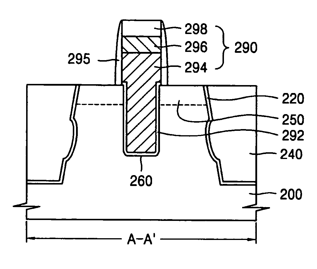
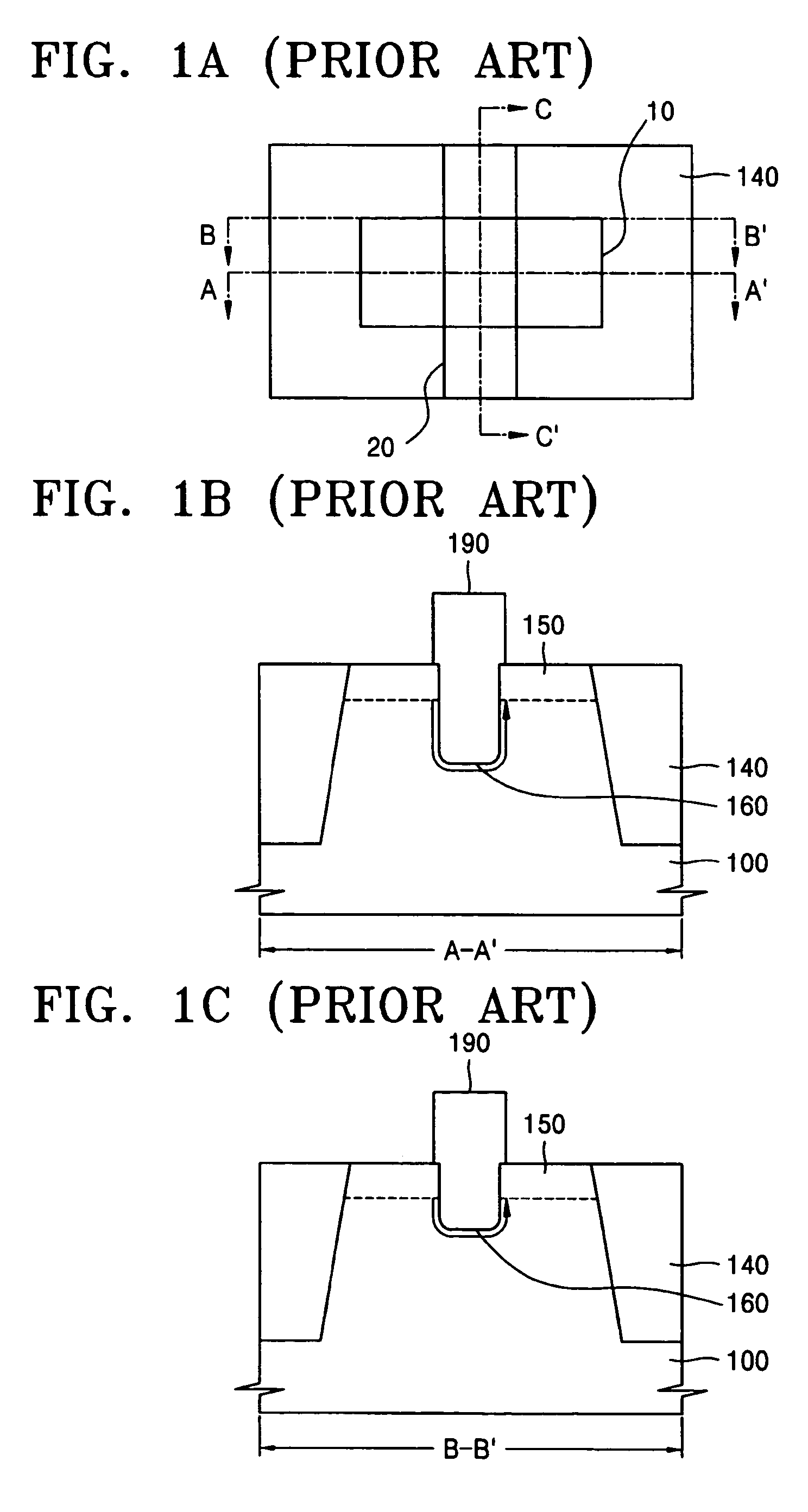
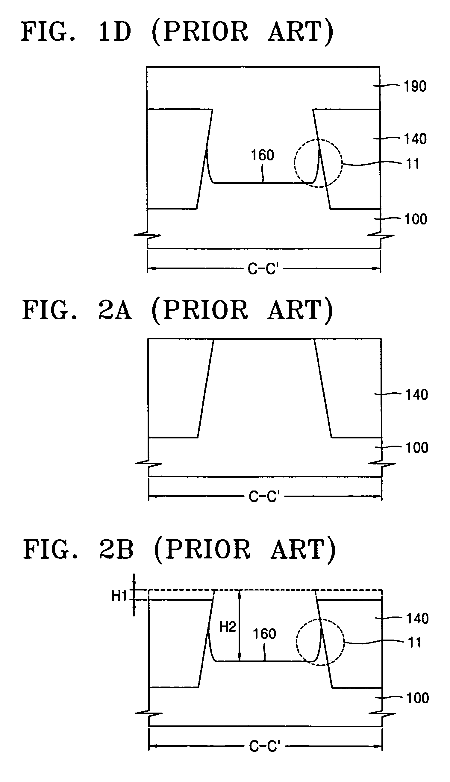
[0029]FIG. 3 is a cross-sectional view showing a STI structure and a recess channel trench formed in an active region defined by the STI structure according to one embodiment of the present invention. FIG. 3 is a cross-sectional view of a layout similar to that shown in FIG. 1a, taken along line C–C′.

[0030]Referring to FIG. 3, a STI liner 220 and an insulating layer 240 ...


PUM


Abstract

A shallow trench isolation (STI) structure and a method of forming the STI structure. The STI structure defines an active region formed with a recess channel transistor. The STI structure includes a STI trench has a laterally curved rounding portion on the bottom of the recess channel trench. In order to form the STI trench with the rounding portion, a semiconductor substrate is selectively and anisotropically dry etched to form the trench. Then, the semiconductor substrate is isotropically etched around the bottom height of the recess channel trench to form the rounding portion, and then further anisotropically dry etched, thereby forming the STI trench. After an insulating layer that fill the STI trench is formed on the resultant structure, an upper surface of the resultant structure is planarized to expose a surface of the semiconductor substrate.

Description

BACKGROUND OF THE INVENTION[0001]This application claims the priority of Korean Patent Application No. 2003-73836, filed on Oct. 22, 2003, in the Korean Intellectual Property Office, the disclosure of which is incorporated herein by reference in its entirety.[0002]1. Field of the Invention[0003]The present invention relates to semiconductor integrated circuits and to a method of forming the same, and more particularly to a shallow trench isolation (STI) structure for recess channel transistors and a method of making the same.[0004]2. Description of the Related Art[0005]Increased packing density makes isolation techniques that electrically isolate mutually adjacent devices very important. Shallow trench isolation (STI) is a device isolation technique. In STI, a trench that defines an active region is formed in a semiconductor substrate. Then, the inside of the trench (i.e. the STI trench) is filled with an insulating material to form an isolating layer. Generally, the STI trench has ...

Claims


Application Information

Patent Timeline
Patent Type & Authority Patents(United States)
IPC IPC(8): H01L21/76H01L21/762H01L21/8242
CPCH01L21/76232H01L27/10876H10B12/053H01L21/762
Inventor PARK
Owner SAMSUNG ELECTRONICS CO LTD
Why Eureka
Try Eureka