Sense amplifier bitline boost circuit

a boost circuit and amplifier technology, applied in the field of magnetoresitive memory devices, can solve the problems of loss of stored data, increased cost, and increased cost, and achieve the effect of reducing manufacturing cost and increasing memory density

Active Publication Date: 2007-01-09
INFINEON TECH AG
View PDF4 Cites 68 Cited by
  • Summary
  • Abstract
  • Description
  • Claims
  • Application Information

AI Technical Summary

Benefits of technology

[0016]In one aspect, the present invention relates to utilizing the resistance characteristics of MTJ devices, including devices based on GMR or another mechanism in which a resistance is dependent on the direction of polarization of a free magnetic layer with respect to a fixed magnetic layer, that can exhibit distinct resistance values dependent on the magnetic orientation of a magnetic layer so that digital data can be stored and read. In response to the need to quickly alter the charge in parasitic capacitance in the circuit during the cell sensing process while providing a fixed voltage to the cell when the cell resistance is being sensed, the present invention provides a bitline boost circuit to increase the available current to charge parasitic capacitance. The bitline boost circuit is configured so that substantially the same voltage is provided to the cell while it is being sensed as the original circuit, and additional current is provided during an initial cell resistance sensing period to charge parasitic capacitance. Thereby the design of high density and low cost MTJ memory devices is enabled which can be read reliably with increased speed.
[0017]Embodiments of the present invention achieve technical advantages by configuring a current sense amplifier to sense the resistance of a memory cell with a bitline boost circuit. The current sense amplifier includes a voltage comparator having a first input, a second input, and an output, and a current mirror coupled between the first and second inputs of the voltage comparator. The output of the voltage comparator indicates the logic state of the memory cell. The current sense amplifier also includes first and second clamping devices coupled between the first and second inputs of the voltage comparator and a first node and a second node conducting first and second input signals, respectively, to the current sense amplifier. The first and second clamping devices of the current sense amplifier are coupled to a reference voltage. The bitline boost circuit is configured to clamp the voltage of the first signal at substantially the same level as the first clamping device. The bitline boost circuit is also configured to provide a current to the node conducting the first signal during an initial period of sensing the resistance of the memory cell. The bitline boost circuit includes a source follower coupled to the reference voltage and a switch coupled to a voltage source. The source follower includes a source, a gate, and a drain, the gate being coupled to the reference voltage and the gate being coupled to the first signal. The drain of the source follower is coupled to the switch. The switch is controlled to conduct during an initial period of sensing the resistance of a memory cell, thereby providing current to the source follower to charge circuit parasitic capacitance. Preferably, the source follower is configured with an n-type MOSFET and the switch is configured with a p-type MOSFET. The resulting current sense amplifier can be used to implement a memory device with fast read times and that can be manufactured with low cost.
[0018]In accordance with another preferred embodiment of the present invention a memory device is configured with a current sense amplifier that senses the resistance of memory cells using a bitline boost circuit. The current sense amplifier includes a voltage comparator having a first input, a second input, and an output, and a current mirror coupled between the first and second inputs of the voltage comparator. The output of the voltage comparator signals the logic state of the memory cell. The current sense amplifier also includes first and second clamping devices coupled between the first and second inputs of the voltage comparator and a first node and a second node conducting first and second input signals, respectively, to the current sense amplifier. The first and second clamping devices of the current sense amplifier are coupled to a reference voltage. The bitline boost circuit is configured to clamp the voltage of the first signal at substantially the same level as the first clamping device. The bitline boost circuit is also configured to provide a current to the node conducting the first signal during an initial period of sensing the resistance of the memory cell. The bitline boost circuit includes a source follower coupled to the reference voltage and a switch coupled to a voltage source. The source follower includes a source, a gate, and a drain, the gate being coupled to the reference voltage and the gate being coupled to the first signal. The drain of the source follower is coupled to the switch. The switch is controlled to conduct during an initial period of sensing the resistance of a memory cell, thereby providing current to the source follower to charge circuit parasitic capacitance. Preferably, the source follower is configured with an n-type MOSFET and the switch is configured with a p-type MOSFET. Preferably, the memory device is configured with MTJ cells. The resulting memory device can provide fast read times and can be manufactured with low cost.
[0019]Another embodiment of the present invention is a method of configuring a current sense amplifier to sense the resistance of a memory cell with a bitline boost circuit. The method includes configuring the current sense amplifier with a voltage comparator having a first input, a second input, and an output, and a current mirror coupled between the first and second inputs of the voltage comparator. The method includes configuring the output of the voltage comparator to signal the logic state of the memory cell. The method includes configuring the current mirror to supply a current to the second node that is proportional to the current in the first node. The method also includes configuring the current sense amplifier with first and second clamping devices coupled between the first and second inputs of the voltage comparator and configuring a first node and a second node to conduct first and second input signals, respectively, to the current sense amplifier. The method also includes coupling the first and second clamping devices of the current sense amplifier to a reference voltage. The method further includes configuring the first clamping device so that it clamps a voltage of the node conducting the first signal to a voltage related to the reference voltage. The method further includes configuring the second clamping device so that it clamps a voltage of the node conducting the second signal to substantially the same level as the first clamping device. The method further includes configuring the bitline boost circuit to clamp the voltage of the first signal at substantially the same level as the first clamping device. The method includes configuring the bitline boost circuit to provide a current to the node conducting the first signal during an initial period of sensing the resistance of the memory cell. The method includes providing the bitline boost circuit with a source follower and coupling it to the reference voltage, and then coupling a switch to a voltage source. The method includes configuring the source follower with a source, a gate, and a drain, coupling the gate to the reference voltage and coupling the gate to the first signal. The method further includes coupling the drain of the source follower to the switch. The method includes controlling the switch to conduct during an initial period of sensing the resistance of a memory cell, and providing thereby current to the source follower to charge circuit parasitic capacitance. The method includes providing a second source follower to clamp the node conducting the second signal to the same voltage as the first clamping device clamps the node conducting the first signal. Preferably, the method includes configuring the source follower with an n-type MOSFET and configuring the switch with a p-type MOSFET. The resulting current sense amplifier can be used to implement a memory device with fast read times and low manufacturing cost.
[0022]Embodiments of the present invention achieve technical advantages as a memory device including MTJ cells storing digital data. Advantages of embodiments of the present invention include a memory device with increased memory density and reduced manufacturing cost, that is non-volatile upon removal of electrical power, and that does not require its data to be re-written after it has been read.

Problems solved by technology

DRAMs have moderate cost, are very fast and can have access times on the order of a few nanoseconds, but lose the stored data upon loss of electrical power, i.e., they are “volatile.” Present “flash” memories are non-volatile, are more expensive perhaps by a factor of ten, and have access times near a microsecond.
Further application considerations for each technology include limitations on the number of times a memory cell can be written or read before it deteriorates, how long it reliably retains data, its data storage density, how much energy it consumes, the need for integral mechanical devices such as for disk drives and tapes, and the complexity and expense of associated circuitry.
In addition, memory devices based on charge storage generally need to be rewritten each time they are read, adding to their complexity and cost.
Considering these limitations, there is now no ideal technology for general applications.
However, a limitation of a magnetic tunnel junction cell resistance sensing process as described above is the time required to charge parasitic circuit capacitance when sensing its programmed state.
Since circuit voltage settling time is inversely proportional to the available capacitance charging current, these prior art circuits limit the speed at which cell resistance can be sensed.

Method used


Image

  • Sense amplifier bitline boost circuit
  • Sense amplifier bitline boost circuit
  • Sense amplifier bitline boost circuit

Examples


Embodiment Construction

[0037]The making and using of the presently preferred embodiments are discussed in detail below. It should be appreciated, however, that the present invention provides many applicable inventive concepts that can be embodied in a wide variety of specific contexts. The specific embodiments discussed are merely illustrative of specific ways to make and use the invention, and do not limit the scope of the invention.

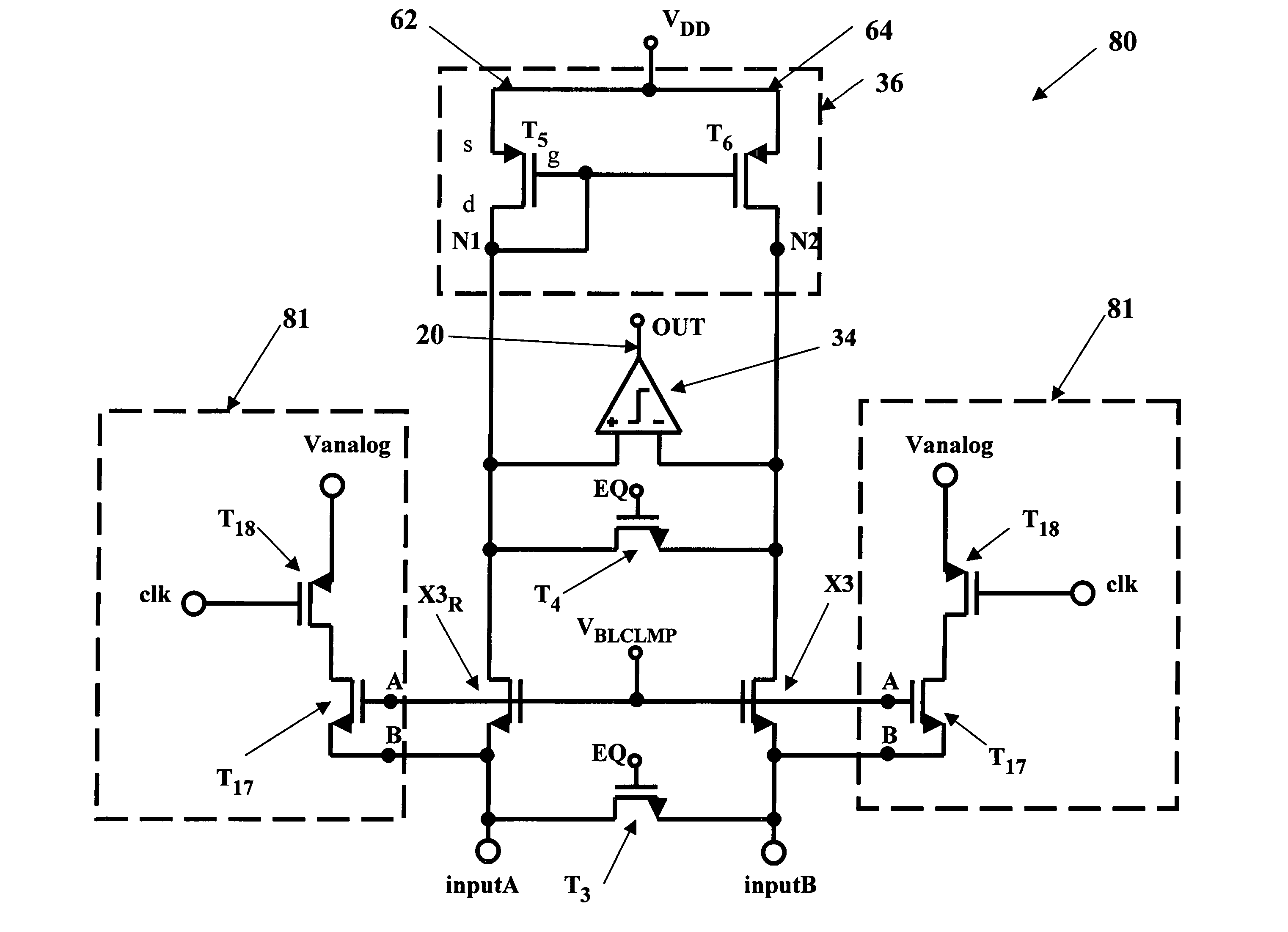
[0038]Embodiments of the present invention will be described with respect to preferred embodiments in a specific context, namely a FET MRAM device configured with a circuit to provide increased current to charge circuit parasitic capacitance during a cell resistance sensing interval to increase the speed at which a resistive state of a memory cell may be sensed. The invention may be applied to resistive memory devices and other memory devices that include a plurality of current sense amplifiers and reference current sources to detect the resistive state of MRAM memory cells c...


PUM


Abstract

A current sense amplifier including clamping devices and a current mirror is configured to sense the resistance of an MTJ memory cell utilizing a bitline boost circuit to shorten the charging time for parasitic circuit capacitance. The bitline boost circuit includes a source follower coupled to a reference voltage and a switch coupled to another voltage source. The switch is enabled to conduct during an initial period of sensing the resistance of the memory cell. The source follower in the bitline boost circuit is configured to clamp the voltage of an input signal at substantially the same level as the clamping devices, and to provide additional current to shorten the period for charging parasitic capacitance. The resulting current sense amplifier can be used to implement a memory device with fast and reliable read times and low manufacturing cost.

Description

CROSS-REFERENCE TO RELATED APPLICATIONS[0001]The following U.S. patents and / or commonly assigned patent applications are hereby incorporated herein by reference:[0002]U.S. Pat. No. orU.S. Application Ser. No.Filing DateIssue Date6,946,882Dec. 20, 2002Sep. 20, 200510 / 937,155Sep. 7, 200410 / 982,026Nov. 4, 200410 / 925,487Aug. 25, 2004TECHNICAL FIELD[0003]Embodiments of the present invention relate generally to a magnetoresitive memory device and the preferred embodiment relates more particularly to using a bitline boost circuit to decrease the time required to charge parasitic circuit capacitance when sensing the programmed state of a magnetic random access memory cell.BACKGROUND[0004]Semiconductors are used in integrated circuits for electronic applications, including radios, televisions, cell phones, and personal computing devices, as examples. One type of semiconductor device is a semiconductor storage device, such as a dynamic random access memory (DRAM) and flash memory, which uses ...

Claims


Application Information

Patent Timeline
Patent Type & Authority Patents(United States)
IPC IPC(8): G11C7/02G11C7/00
CPCG11C5/145G11C7/06G11C11/16G11C7/12G11C2207/063
Inventor GOGL, DIETMARVIEHMANN, HANS-HEINRICH
Owner INFINEON TECH AG
Why Eureka
Try Eureka