[0015] In one aspect, the present invention relates to utilizing the resistance characteristics of MTJ devices, including devices based on GMR or another mechanism in which a resistance is dependent on the direction of polarization of a free
magnetic layer with respect to a fixed
magnetic layer, that can exhibit distinct resistance values dependent on the
magnetic orientation of a
magnetic layer so that
digital data can be stored and read. In response to the need to quickly alter the charge in
parasitic capacitance in the circuit during the cell sensing process while providing a fixed voltage to the cell when the
cell resistance is being sensed, the present invention provides a bitline boost circuit to increase the available current to charge
parasitic capacitance. The bitline boost circuit is configured so that substantially the same voltage is provided to the cell while it is being sensed as the original circuit, and additional current is provided during an
initial cell resistance sensing period to charge parasitic capacitance. Thereby the design of
high density and low cost MTJ memory devices is enabled which can be read reliably with increased speed.
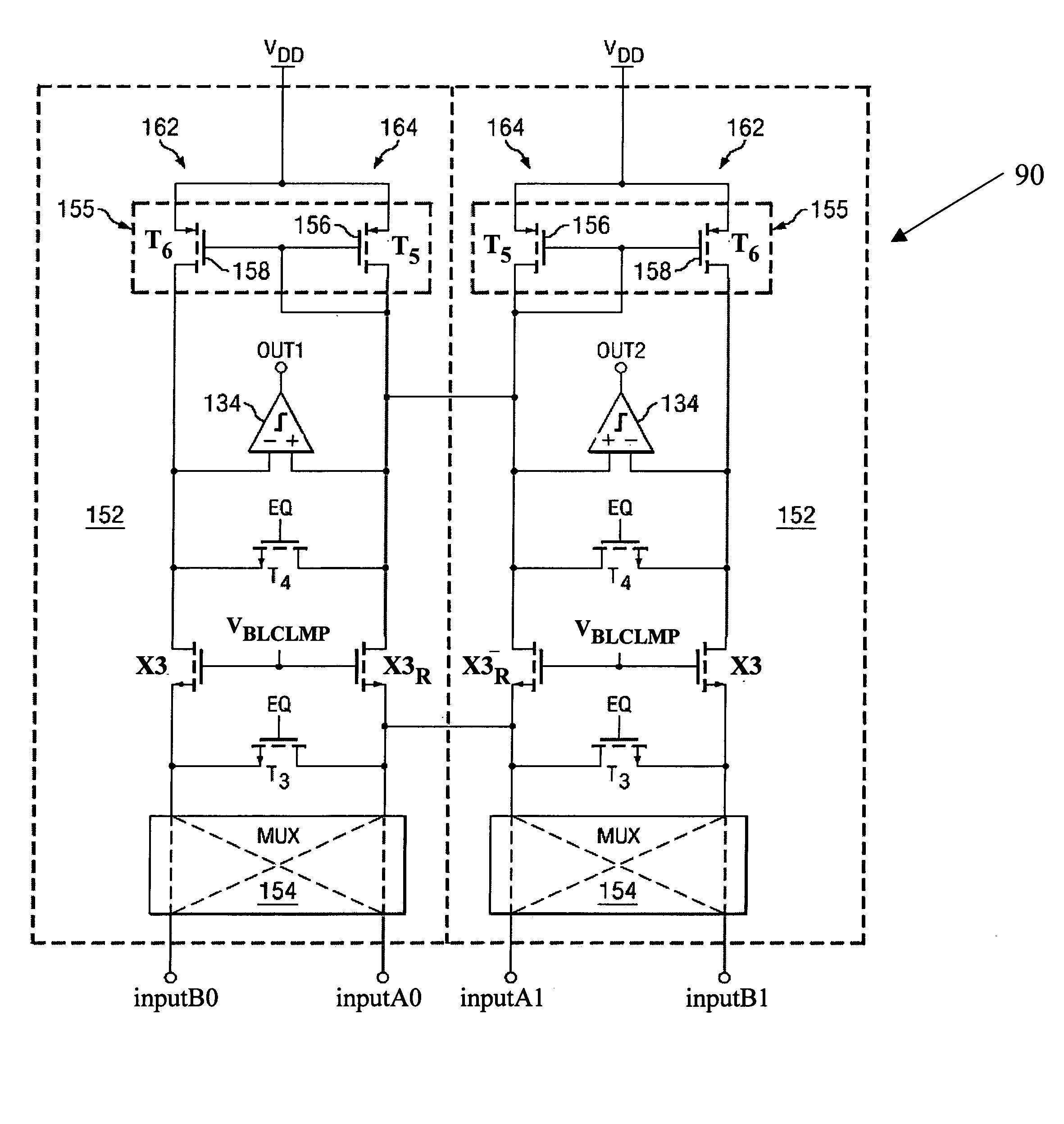
[0016] Embodiments of the present invention achieve technical advantages by configuring a
current sense amplifier to sense the resistance of a memory cell with a bitline boost circuit. The current
sense amplifier includes a voltage
comparator having a first input, a second input, and an output, and a
current mirror coupled between the first and second inputs of the voltage
comparator. The output of the voltage
comparator indicates the
logic state of the memory cell. The current
sense amplifier also includes first and second clamping devices coupled between the first and second inputs of the voltage comparator and a first node and a second node conducting first and second input signals, respectively, to the current
sense amplifier. The first and second clamping devices of the current sense
amplifier are coupled to a reference voltage. The bitline boost circuit is configured to clamp the voltage of the first
signal at substantially the same level as the first clamping device. The bitline boost circuit is also configured to provide a current to the node conducting the first
signal during an initial period of sensing the resistance of the memory cell. The bitline boost circuit includes a source follower coupled to the reference voltage and a switch coupled to a
voltage source. The source follower includes a source, a gate, and a drain, the gate being coupled to the reference voltage and the gate being coupled to the first signal. The drain of the source follower is coupled to the switch. The switch is controlled to conduct during an initial period of sensing the resistance of a memory cell, thereby providing current to the source follower to charge circuit parasitic capacitance. Preferably, the source follower is configured with an n-type
MOSFET and the switch is configured with a p-type
MOSFET. The resulting current sense
amplifier can be used to implement a memory device with fast read times and that can be manufactured with low cost.
[0017] In accordance with another preferred embodiment of the present invention a memory device is configured with a current sense
amplifier that senses the resistance of memory cells using a bitline boost circuit. The current sense amplifier includes a voltage comparator having a first input, a second input, and an output, and a
current mirror coupled between the first and second inputs of the voltage comparator. The output of the voltage comparator signals the
logic state of the memory cell. The current sense amplifier also includes first and second clamping devices coupled between the first and second inputs of the voltage comparator and a first node and a second node conducting first and second input signals, respectively, to the current sense amplifier. The first and second clamping devices of the current sense amplifier are coupled to a reference voltage. The bitline boost circuit is configured to clamp the voltage of the first signal at substantially the same level as the first clamping device. The bitline boost circuit is also configured to provide a current to the node conducting the first signal during an initial period of sensing the resistance of the memory cell. The bitline boost circuit includes a source follower coupled to the reference voltage and a switch coupled to a
voltage source. The source follower includes a source, a gate, and a drain, the gate being coupled to the reference voltage and the gate being coupled to the first signal. The drain of the source follower is coupled to the switch. The switch is controlled to conduct during an initial period of sensing the resistance of a memory cell, thereby providing current to the source follower to charge circuit parasitic capacitance. Preferably, the source follower is configured with an n-type
MOSFET and the switch is configured with a p-type MOSFET. Preferably, the memory device is configured with MTJ cells. The resulting memory device can provide fast read times and can be manufactured with low cost.
[0018] Another embodiment of the present invention is a method of configuring a current sense amplifier to sense the resistance of a memory cell with a bitline boost circuit. The method includes configuring the current sense amplifier with a voltage comparator having a first input, a second input, and an output, and a current mirror coupled between the first and second inputs of the voltage comparator. The method includes configuring the output of the voltage comparator to signal the
logic state of the memory cell. The method includes configuring the current mirror to supply a current to the second node that is proportional to the current in the first node. The method also includes configuring the current sense amplifier with first and second clamping devices coupled between the first and second inputs of the voltage comparator and configuring a first node and a second node to conduct first and second input signals, respectively, to the current sense amplifier. The method also includes
coupling the first and second clamping devices of the current sense amplifier to a reference voltage. The method further includes configuring the first clamping device so that it clamps a voltage of the node conducting the first signal to a voltage related to the reference voltage. The method further includes configuring the second clamping device so that it clamps a voltage of the node conducting the second signal to substantially the same level as the first clamping device. The method further includes configuring the bitline boost circuit to clamp the voltage of the first signal at substantially the same level as the first clamping device. The method includes configuring the bitline boost circuit to provide a current to the node conducting the first signal during an initial period of sensing the resistance of the memory cell. The method includes providing the bitline boost circuit with a source follower and
coupling it to the reference voltage, and then
coupling a switch to a
voltage source. The method includes configuring the source follower with a source, a gate, and a drain, coupling the gate to the reference voltage and coupling the gate to the first signal. The method further includes coupling the drain of the source follower to the switch. The method includes controlling the switch to conduct during an initial period of sensing the resistance of a memory cell, and providing thereby current to the source follower to charge circuit parasitic capacitance. The method includes providing a
second source follower to clamp the node conducting the second signal to the same voltage as the first clamping device clamps the node conducting the first signal. Preferably, the method includes configuring the source follower with an n-type MOSFET and configuring the switch with a p-type MOSFET. The resulting current sense amplifier can be used to implement a memory device with fast read times and low manufacturing cost.
[0021] Embodiments of the present invention achieve technical advantages as a memory device including MTJ cells storing
digital data. Advantages of embodiments of the present invention include a memory device with increased memory density and reduced manufacturing cost, that is non-volatile upon removal of electrical power, and that does not require its data to be re-written after it has been read.

