Optical module

a technology of optical modules and optical elements, applied in the field of optical modules, can solve the problems of bulky and expensive optical modules, and achieve the effect of simplifying manufacturing processes

Inactive Publication Date: 2007-01-23
MITSUBISHI ELECTRIC CORP
View PDF26 Cites 1 Cited by
  • Summary
  • Abstract
  • Description
  • Claims
  • Application Information

AI Technical Summary

Benefits of technology

[0010]The present invention has been made to solve the above problems and an object thereof is to provide an optical module able to eliminate the PD carrier and simplify the manufacturing process.
[0034]As described above, according to the present invention, since the electrode which detects emitted light from the radiative device is electrically connected to the wiring patterns and is provided with the conductive coupling member so as to secure the detecting device to the base, the detecting device can be mounted without relying on the PD carrier. As a result, this simplifies manufacturing processes.

Problems solved by technology

The conventional optical module thus configured as above involves numerous troublesome wire bonding processes required for manufacturing of an optical module.
Thus, this requirement invites a bulky and costly optical module, and asks for an additional mounting process for the PD carrier 5.

Method used


Image

  • Optical module
  • Optical module
  • Optical module

Examples


first embodiment

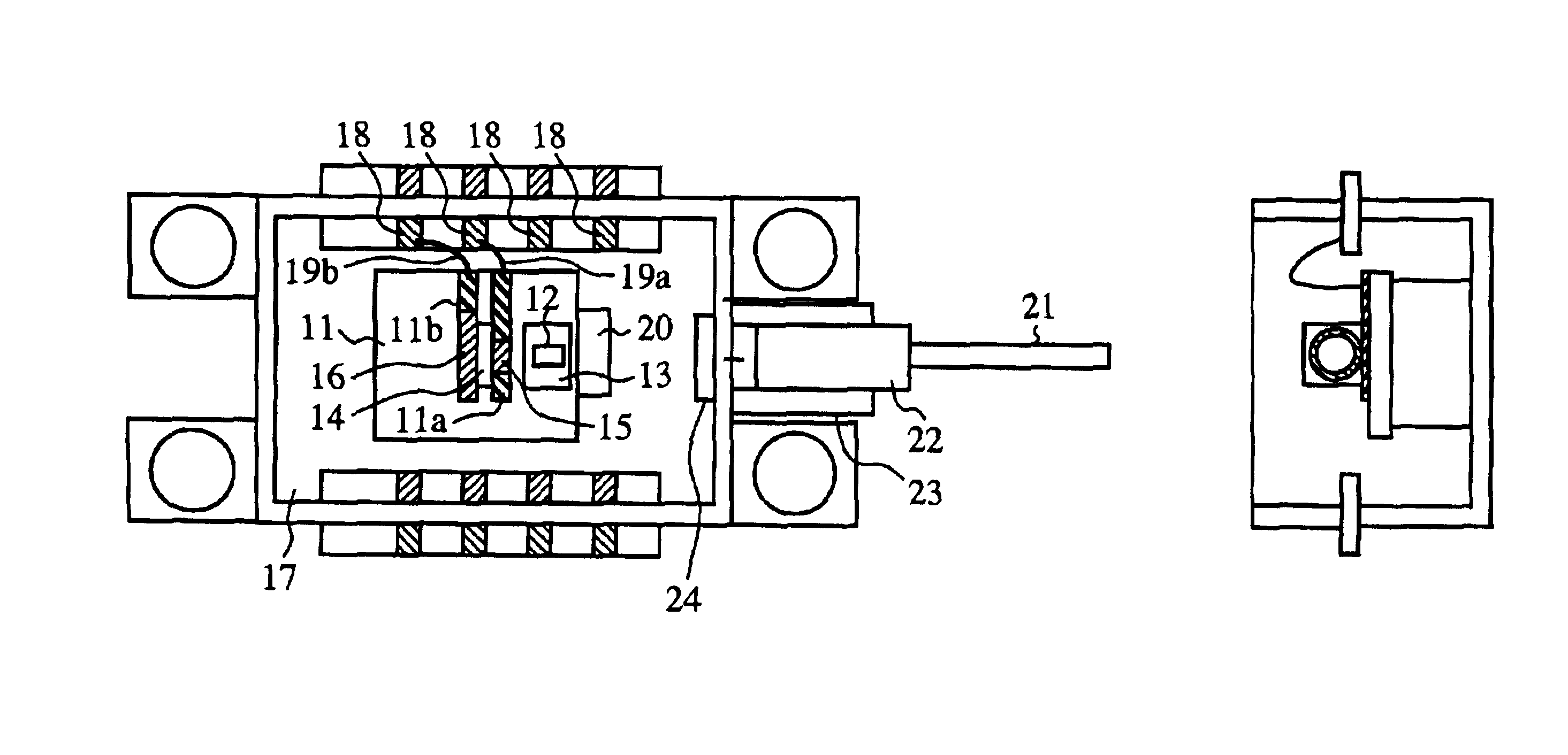
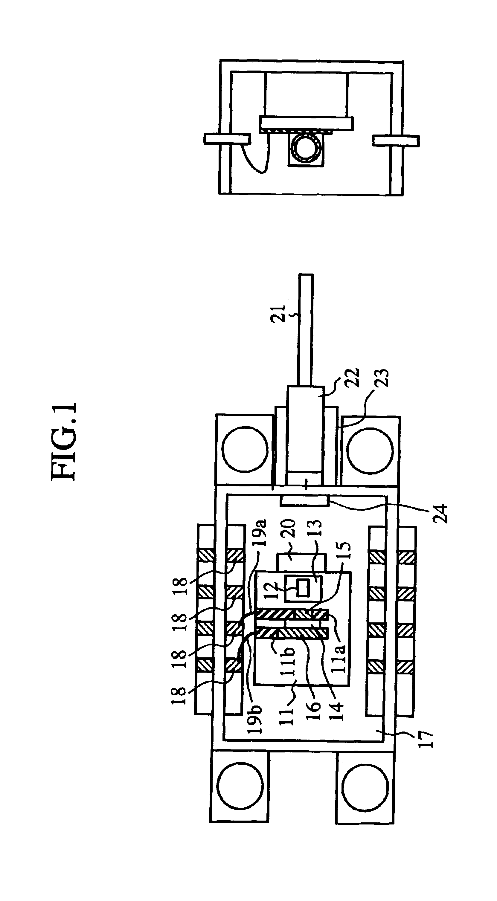
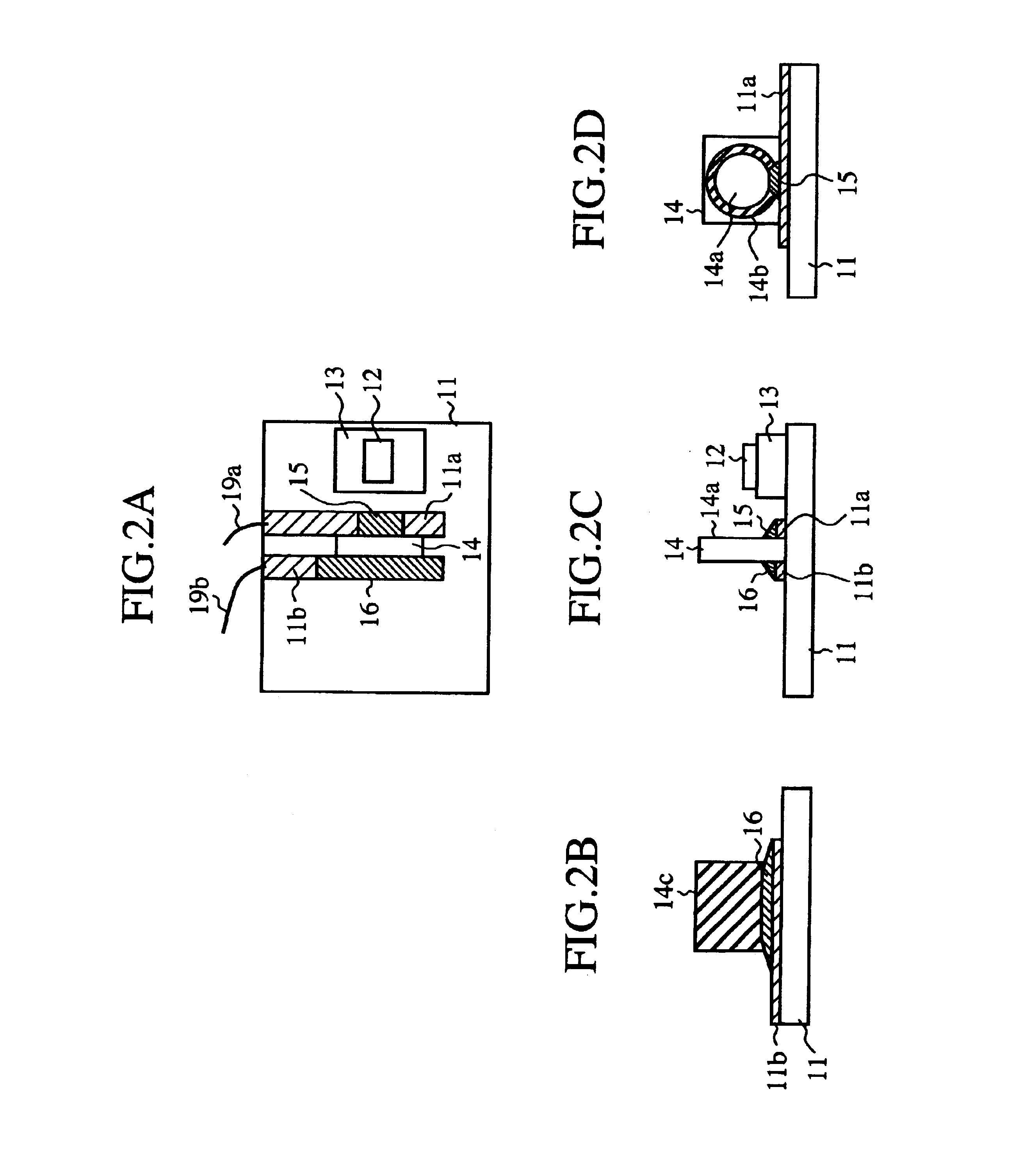
[0093]FIG. 1 is an overall block diagram showing an optical module according to the first embodiment of the present invention. FIG. 2A is a top view showing a purview of an optical module according to the first embodiment. FIG. 2B is a rear view showing a PD element. FIG. 2C is a side view showing a purview of an optical module. FIG. 2D is a front view showing a PD element.

[0094]Referring now to FIG. 1, FIGS. 2A through 2D, reference numeral 11 denotes a dielectric substrate (base) on which wiring patterns 11a, 11b are laid out, 12 an LD element (radiative device) for emitting light to an optical fiber 21, 13 an LD carrier for holding thereon the LD element 12, 14 a PD element (photo detector) for detecting back light (emitted light) emitted from the LD element 12, 14a an incident surface of the PD element 14, 14b an anode electrode provided at the periphery of the photo detector 14a, 14c a cathode electrode provided on the back of the PD element 14.

[0095]Reference numeral 15 denote...

second embodiment

[0107]In the first embodiment, the optical fiber 21 is secured to the package 17, but, as shown in FIG. 4, a receptacle (holding means) may be provided, as an alternative, in the package 17 for removably holding the ferrule 22 by which the optical fiber 21 is fixed. This connects and disconnects the optical fiber 21 to / from the optical fiber at need.

[0108]FIG. 4 is an overall block diagram showing an optical module according to the second embodiment of the present invention.

[0109]Referring to FIG. 4, reference numeral 27 denotes a space into which the ferrule 22 is inserted, 28 a hole with which an optical path is formed.

[0110]FIG. 5 is an overall block diagram showing an optical module according to the second embodiment.

[0111]Referring to FIG. 5, reference numeral 5 denotes a sealing compound.

[0112]Also, in the first embodiment, the lens 20 is placed between the LD element 12 and the optical fiber 21. However, as shown in FIG. 5, the lens 20 is not mandatory.

third embodiment

[0113]FIG. 6 is an overall block diagram showing an optical module according the third embodiment of the present invention. FIG. 7A is a top view showing a purview of an optical module according to the third embodiment. FIG. 7B is a rear view showing a PD element. FIG. 7C is a side view showing a purview of an optical module. FIG. 7D is a front view showing a PD element. IN FIG. 6, FIGS. 7A through 7D, the same reference numerals as those in FIGS. 2, 5 indicate identical or equivalent parts and therefore descriptions thereof are omitted for brevity s sake. Referring to FIG. 6, FIGS. 7A through 7B, reference numeral 30 denotes an optical fiber carrier for holding thereon the optical fiber.

[0114]The operation of the third embodiment will then be described.

[0115]In the first embodiment, the PD element 14 detects front light or back light emitted from the LD element 12. Alternatively, when the optical module is not used as a PD module but as a PD monitor, the PD module 14 may detect emi...


PUM


Abstract

This optical module includes solder which solders an anode electrode of a PD element for detecting back light emitted from an LD element and wiring patterns, and solder which solders a cathode electrode and wiring patterns.

Description

BACKGROUND OF THE INVENTION[0001]1. Field of the Invention[0002]This invention relates to an optical module on which a radiative device and a photo detector for detecting emitted light or the like are mounted.[0003]2. Description of Related Art[0004]FIG. 22A is atop view showing a conventional optical module. FIG. 22B is a side view showing a conventional optical module. FIG. 22C is a front view showing a PD element.[0005]Referring to FIGS. 22A through 22C, reference numeral 1 denotes a substrate on which an LD carrier 3 and a PD carrier are mounted, 2 a radiative device (hereinafter referred to as an LD element, not shown), 3 an LD carrier for holding thereon the LD element 2, 4 a photo detector (hereinafter referred to as a PD element) for detecting back light from the LD element 2, 4a an incident surface of the PD element, at the peripheral of which an anode electrode 4b is provided, and on the opposite surface of which a cathode electrode is provided. Reference numeral 5 denotes...

Claims


Application Information

Patent Timeline
Patent Type & Authority Patents(United States)
IPC IPC(8): G02B6/36G02B6/42H01L31/02H01L31/0203H01L31/0232H01L31/105H01L31/12H01S5/022
CPCG02B6/4201H01L31/02002H01L31/0203H01L31/105H01L31/12G02B6/4292H01L2224/48091H01L2924/00014
Inventor TAKAGI, SHINICHI
Owner MITSUBISHI ELECTRIC CORP
Why Eureka
Try Eureka