
Circuit substrate and electronic equipment

a technology of electronic equipment and circuit substrate, which is applied in the direction of final product manufacturing, sustainable manufacturing/processing, and semiconductor/solid-state device details. it can solve the problems of unfavorable use, increase the operating speed of the semiconductor chip, and the cost of a board, so as to reduce the noise to a sufficient level

Inactive Publication Date: 2007-01-23
FUJITSU LTD
View PDF7 Cites 2 Cited by
  • Summary
  • Abstract
  • Description
  • Claims
  • Application Information

AI Technical Summary

Benefits of technology

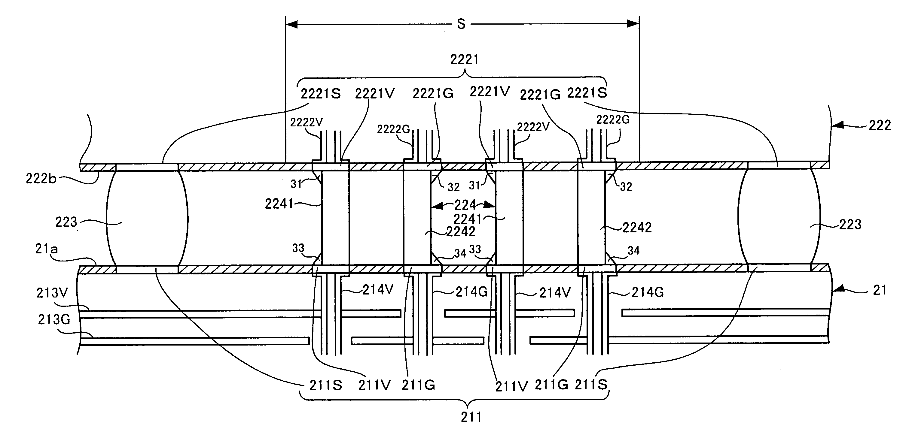
[0021]According to the circuit substrate of the present invention as mentioned above, the noise reduction elements are each sandwiched between an area of a second surface of the first substrate over against the first surface of the first substrate and a surface of the second substrate facing the second surface of the first substrate, and thus the noise reduction elements are disposed in the vicinity of the circuit elements. This feature makes it possible to enhance a noise reduction factor by the noise reduction elements. Further, according to the circuit substrate of the present invention, the terminal of the noise reduction element serves as a part of the path of supply of electric power to the circuit elements, and the noise reduction elements are located just below the circuit elements. Thus, this feature makes it possible to shorten the path of supply of electric power to the circuit elements, and thereby preventing generation of a large noise up to a supply of an electric power to the circuit elements. That is, according to the circuit substrate of the present invention, the noise reduction factor by the noise reduction elements is enhanced and generation of a large noise is prevented. Thus, it is possible to reduce noises to the sufficient level.
[0024]An adoption of the ball grid array system makes it possible to narrow arrangement pitches of the signal terminals of the first substrate and the second substrate, and thereby contributing to a densification of mounting of electronic components.
[0029]Thus, also according to the electronic equipment of the present invention, it is possible to reduce noises to a sufficient level.

Problems solved by technology

When the noise reduction elements are disposed on a board, if it is intended that a large number of noise reduction elements are disposed, it would undesirably involve a cost up and large-sizing of a board.
However, an increment of the operating speed of the semiconductor chip needs further reduction of noises without an increment of the number of noise reduction elements.

Method used


Image

  • Circuit substrate and electronic equipment
  • Circuit substrate and electronic equipment
  • Circuit substrate and electronic equipment

Examples


Embodiment Construction

[0035]Hereinafter, there will be explained a personal computer by way of example of an embodiment of electronic equipment of the present invention.

[0036]Embodiments of the present invention will be described with reference to the accompanying drawings.

[0037]FIG. 3 is a perspective view of a personal computer that is an embodiment of electronic equipment of the present invention.

[0038]A personal computer (PC) 10 comprises: a main frame section 11 incorporating therein a CPU (central processing unit), a RAM (random access memory), a hard disk and so on; a display unit for displaying an image and a string of characters on a display screen 12a in accordance with an instruction from the main frame section 11; a keyboard 13 for inputting an instruction of a user to the PC 10; and a mouse 14 for inputting an instruction according to an icon or the like displayed at a designated position on the display screen 12a. The PC 10 corresponds to the electronic equipment of the present invention.

[0...


PUM


Abstract

A circuit substrate comprises a first substrate on a first surface of which circuit elements are loaded, a second substrate on which the first substrate is loaded, and noise reduction elements. Each of the noise reduction elements is sandwiched between an area of a second surface of the first substrate over against the first surface of the first substrate and a surface of the second substrate facing the second surface of the first substrate. The noise reduction element is connected between a power source terminal of the second surface of the first substrate and a power source terminal of the surface of the second substrate, and / or between a ground terminal of the second surface of the first substrate and a ground terminal of the surface of the second substrate.

Description

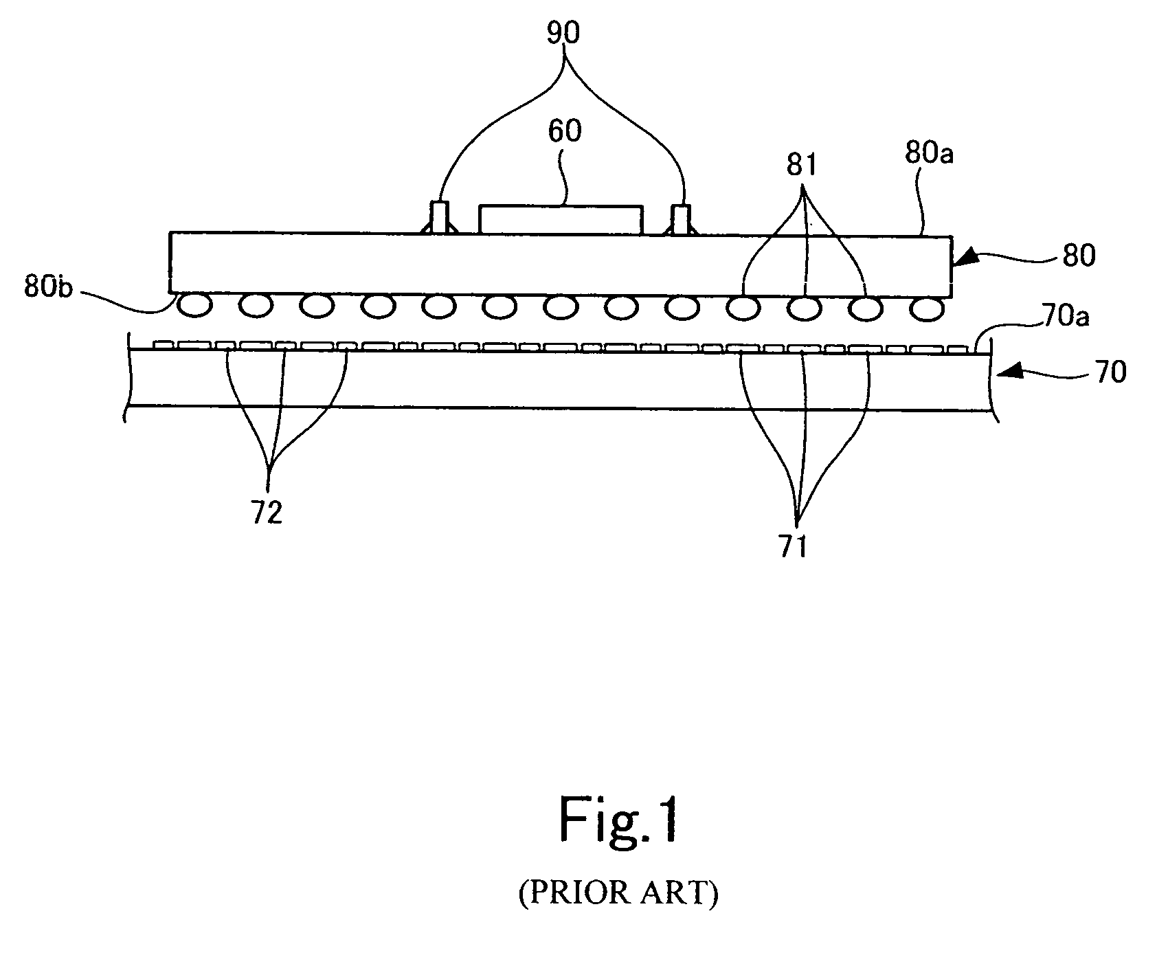
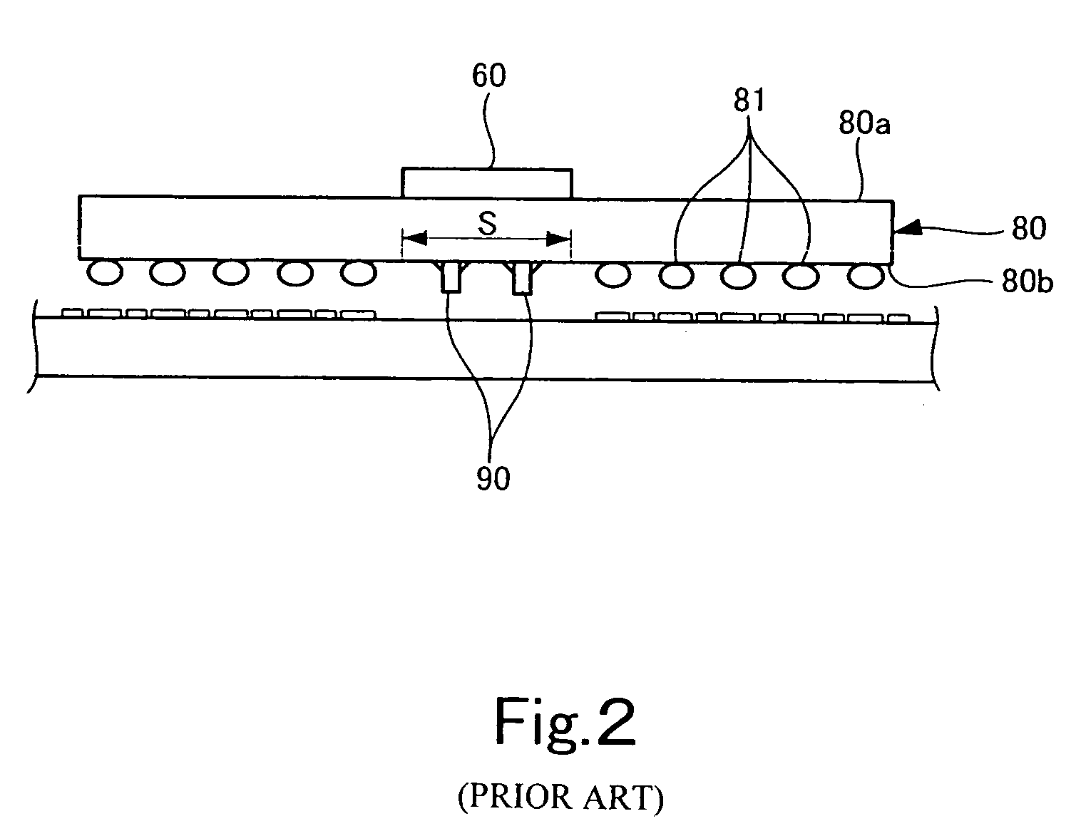
BACKGROUND OF THE INVENTION[0001]1. Field of the Invention[0002]The present invention relates to a circuit substrate having a first substrate that is loaded with circuit elements on a first surface thereof and a second substrate that is loaded with the first substrate, and electronic equipment that is loaded with the circuit substrate and is formed on the circuit substrate.[0003]2. Description of the Related Art[0004]Noise reduction elements for reducing noises between a power source and the ground are provided in the vicinity of a semiconductor chip that is loaded onto a board such as a mother board and a daughter board.[0005]FIG. 1 is a view typically showing a conventional example in which a semiconductor chip is loaded onto a mother board.[0006]According to the conventional example shown in FIG. 1, first, a substrate 80 is prepared in addition to a mother board 70, and a semiconductor chip 60 is mounted on a surface 80a of the additionally prepared substrate 80 and in addition n...

Claims


Application Information

Patent Timeline
Patent Type & Authority Patents(United States)
IPC IPC(8): H05K1/18H05K1/14H01L23/498H01L23/50H05K1/02
CPCH01L23/50H05K1/0231H01L23/49816H01L2224/16H01L2924/15311H01L2924/19105H05K2201/10734H05K1/145H05K2201/10515H05K2201/1053H05K2201/10636H01L2924/19106Y02P70/50
Inventor AIZAWA, OSAMU
Owner FUJITSU LTD
Learn More