Semiconductor device

a technology of semiconductors and devices, applied in the direction of electric variable regulation, process and machine control, instruments, etc., can solve the problems of increased voltage and switching loss during turnoff, increased noise, and increased voltage, so as to achieve marked reduction of power consumption, high efficiency, and lower cost power supply

Inactive Publication Date: 2007-01-23
COLLABO INNOVATIONS INC
View PDF2 Cites 6 Cited by
  • Summary
  • Abstract
  • Description
  • Claims
  • Application Information

AI Technical Summary

Benefits of technology

[0019]When the present invention is employed as a high output switching power supply, a high efficiency switching power supply in which noise from the coil, transformer, and the like, can be markedly suppressed and the power consumption is markedly reduced in comparison with the prior art can be implemented.
[0020]Furthermore, it is possible to implement a smaller, lower cost power supply by integrating the control circuit and switching element on the same semiconductor substrate.
[0021]When the semiconductor device of the present invention is employed as a high output switching power supply, it is possible to implement a highly efficient switching power supply whereby the noise from the coil, transformer and so forth can be markedly suppressed in comparison with the prior art and power consumption is markedly reduced, and a more miniature and low-cost power supply can be implemented by integrating the control circuit and switching element on the same semiconductor substrate. This semiconductor device can be applied to a semiconductor device used in a power supply device such as a switching power supply.

Problems solved by technology

(1) In order to intermittently control the switching element 1 linearly according to the output voltage, the intermittent operating frequency is inputted in the audible range during the switching operation, and hence noise from the transformer, coil, and so forth, which are used for the switching power supply, is generated. Particularly in terms of the output characteristics of the switching power supply, the noise also increases because, when a higher output is required, it is necessary to increase the peak current value (overcurrent detection level) of the IDRAIN determined by the overcurrent detection circuit. When a higher output for the switching power supply is attempted with a conventional semiconductor device, noise from the transformer, coil, and the like, is generated, which represents an obstacle to usage in a high output switching power supply.
(2) When the output of the switching power supply is increased by using a conventional semiconductor device, because the overcurrent detection level must be increased as also mentioned in (1) above, when the output load state is a light load state or loadless state, the increased voltage and the switching loss during turnoff increases. Hence, this is an obstacle to higher efficiency.

Method used


Image

  • Semiconductor device
  • Semiconductor device
  • Semiconductor device

Examples


first embodiment

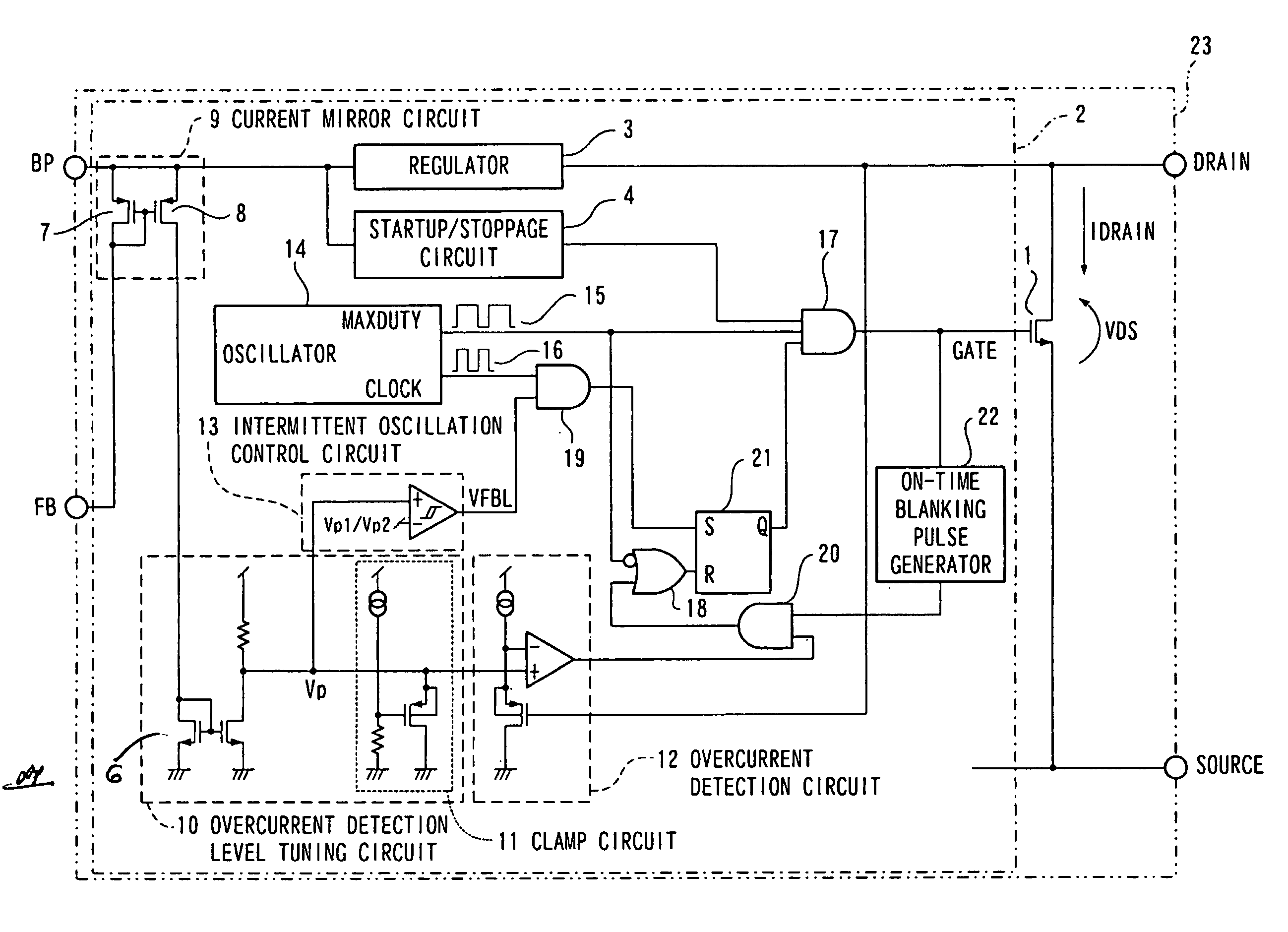
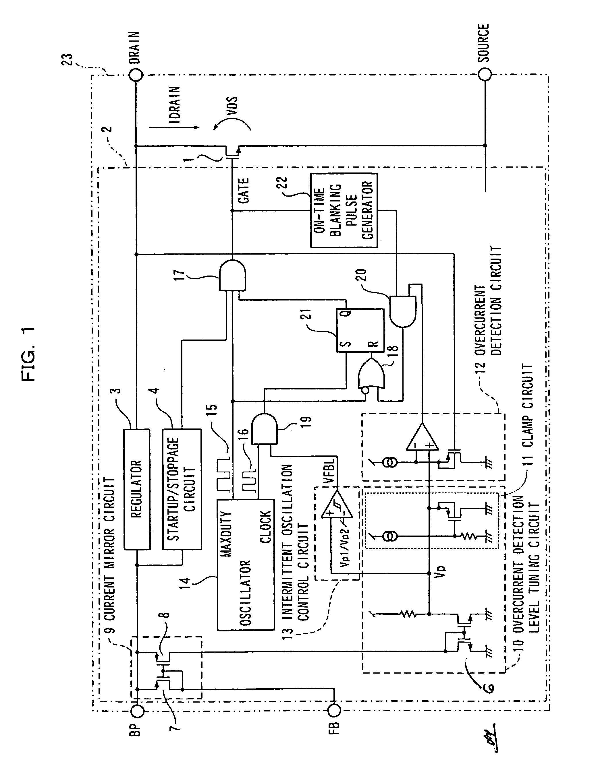
[0029]FIG. 1 is a constitutional view of the semiconductor device of the first embodiment of the present invention.

[0030]In comparison with the conventional example shown in FIG. 5, the semiconductor device of FIG. 1 differs in that a current mirror circuit 9, an overcurrent detection level tuning circuit 10, a clamp circuit 11, an overcurrent detection circuit 12, and an intermittent oscillation control circuit 13 have been added.

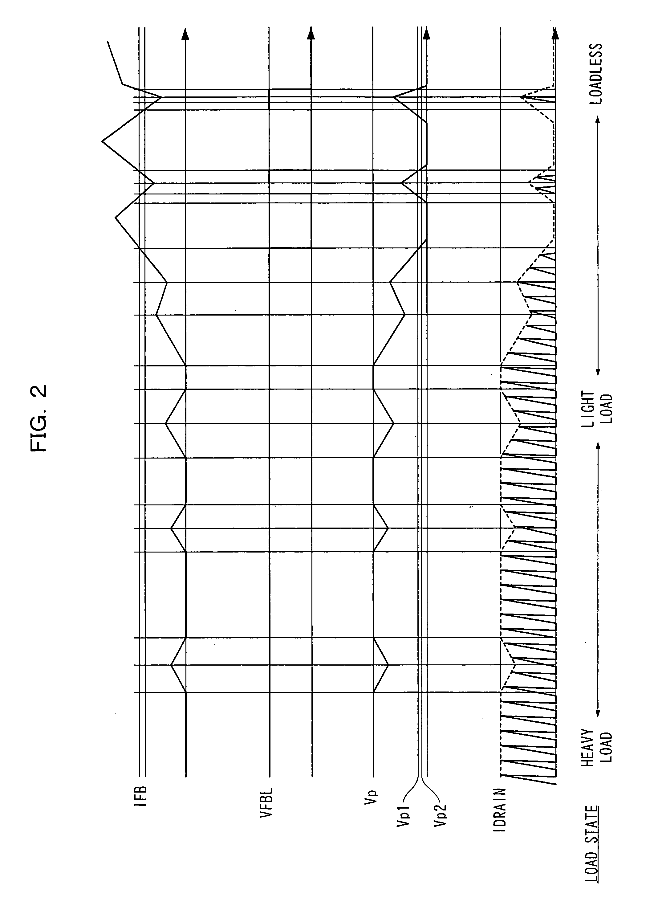
[0031]The operation of the semiconductor device thus constituted will now be described using the operation waveform shown in FIG. 2. IFB in FIG. 2 denotes the FB terminal current of the control circuit 2 in FIG. 1; VFBL denotes the output signal of the intermittent oscillation control circuit 13 in FIG. 1; Vp denotes the terminal voltage connected to the+terminal of the intermittent oscillation control circuit 13; and the IDRAIN denotes the drain current flowing between the DRAIN terminal and SOURCE terminal of the switching element 1.

[0032]The BP terminal...

second embodiment

[0036]FIG. 3 is a constitutional view of the semiconductor device of the second embodiment of the invention. The circuit constitution and operation are also completely the same except for the fact that the overheating protection circuit 24 is added to the semiconductor device of the first embodiment shown in FIG. 1.

[0037]The overheating protection circuit 24 is a circuit for protecting a semiconductor device 23, which comprises the switching element 1 and control circuit 2, from heat emitted by the semiconductor device 23 by means of the ON / OFF control of the switching element 1. Examples of protection afforded by the overheating protection circuit 24 include a latch mode (a mode in which the ON / OFF control of the switching element 1 is completely stopped until this ON / OFF control is cancelled by cancellation means when the temperature exceeds that prescribed), and a self-feedback mode (a mode in which the ON / OFF control of the switching element 1 is stopped when the temperature exc...

third embodiment

[0038]FIG. 4 is a constitutional view of the semiconductor device of the third embodiment of this invention. The semiconductor device of the third embodiment of the present invention shown in FIG. 4 pertains to the overcurrent detection method, and, with regard to the method of detecting the ON voltage of the switching element 1, the semiconductor device of the first embodiment in FIG. 1 has a certain fixed current ratio with the switching element 1, the operation being the same as the first embodiment of the present invention except for being different by virtue of being a method in which a sense MOSFET 25 connected in parallel to the switch element 1 and a sense resistor 26 connected in series to the source terminal of the sense MOSFET 25 are used and the voltage across the terminals of the sense resistor 26 is detected.

[0039]Further, by adding the overheating protection circuit 24 as shown in the second embodiment of the present invention above to the third embodiment of the pres...


PUM


Abstract

The present invention relates to a semiconductor device that is employed in a switching power supply for which a higher output is required, prevents noise from the coil, transformer, and so forth and implements a high efficiency power supply. By connecting a current mirror circuit including a p-type MOSFET, an overcurrent detection level tuning circuit, an overcurrent detection circuit, and an intermittent oscillation control circuit to an FB terminal peripheral circuit that is a feedback signal input terminal, PWM control capable of varying the IDRAIN peak value is implemented for the transition from a heavy load state to a light load state and intermittent oscillation control is implemented for the transition between a light load state to a loadless state, such that noise from the coil, transformer, and the like is suppressed and higher efficiency is realized.

Description

BACKGROUND OF THE INVENTION[0001]1. Field of the Invention[0002]The present invention relates to a semiconductor device employed in a power supply device such as a switching power supply, and relates more particularly to a power-saving technology for a power supply device.[0003]2. Description of the Related Art[0004]FIG. 5 shows a conventional semiconductor device (See U.S. Pat. No. 6,297,623, for example). The conventional semiconductor device is, in a broad classification, constituted by a switching element 1 and a control circuit 2 for controlling the switching element 1.[0005]The switching element 1 is a high withstand voltage power element such as a power MOSFET.[0006]The control circuit 2 comprises a total of five terminals, which are terminals connected to the DRAIN, GATE, and SOURCE terminals of the switching element 1 respectively, a BP terminal, which is a reference voltage terminal of the control circuit 2, and an FB terminal, which is a feedback signal input terminal. A ...

Claims


Application Information

Patent Timeline
Patent Type & Authority Patents(United States)
IPC IPC(8): H02M3/335G05F1/66G05F3/26H02M1/00H02M3/155H02M3/156
CPCH02M3/156H02M1/32Y02B70/16H02M2001/0032H02M1/0032Y02B70/10G05F1/66G05F3/26
Inventor HACHIYA, YOSHIAKI
Owner COLLABO INNOVATIONS INC
Why Eureka
Try Eureka