Method for automatic determination of semiconductor plasma chamber matching and source of fault by comprehensive plasma monitoring

a plasma chamber and comprehensive technology, applied in the direction of material excitation, thermal excitation analysis, electric discharge tube analysis, etc., can solve the problems of insufficient pre-conditioning of the chamber, extended down time can be very costly, and the operator is alarmed

Inactive Publication Date: 2007-01-30
APPLIED MATERIALS INC
View PDF6 Cites 83 Cited by
  • Summary
  • Abstract
  • Description
  • Claims
  • Application Information

AI Technical Summary

Problems solved by technology

If the plasma state of the process and chamber during processing does not match that of a selected process in a “reference” chamber, a potential fault is detected and the operator is alarmed to take appropriate action.
In a semiconductor manufacturing environment, chambers can be found to have insufficient pre-conditioning, such as seasoning, or to have hardware related problems.
Extended down time can be very costly.

Method used


Image

  • Method for automatic determination of semiconductor plasma chamber matching and source of fault by comprehensive plasma monitoring
  • Method for automatic determination of semiconductor plasma chamber matching and source of fault by comprehensive plasma monitoring
  • Method for automatic determination of semiconductor plasma chamber matching and source of fault by comprehensive plasma monitoring

Examples


Embodiment Construction

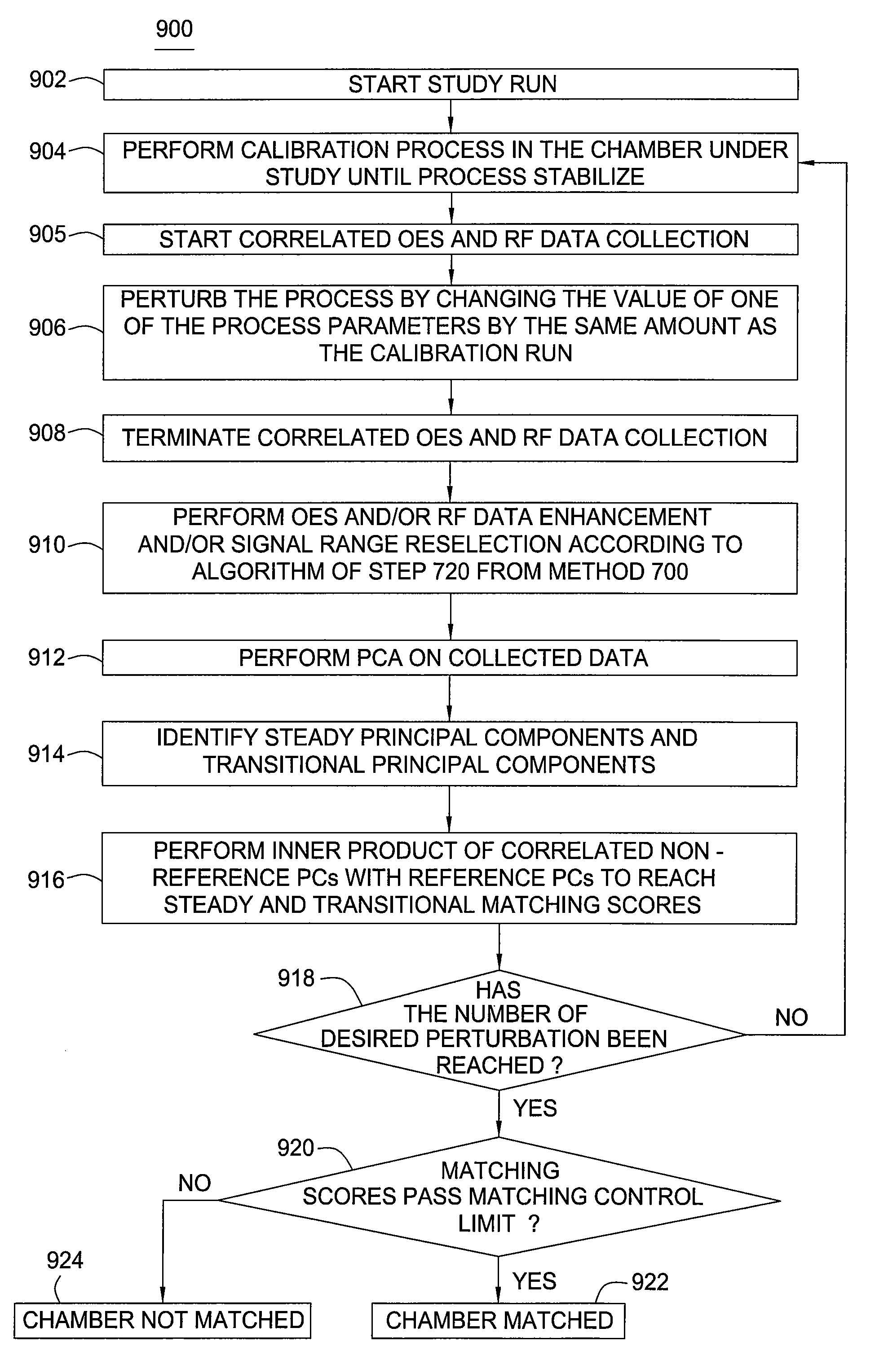
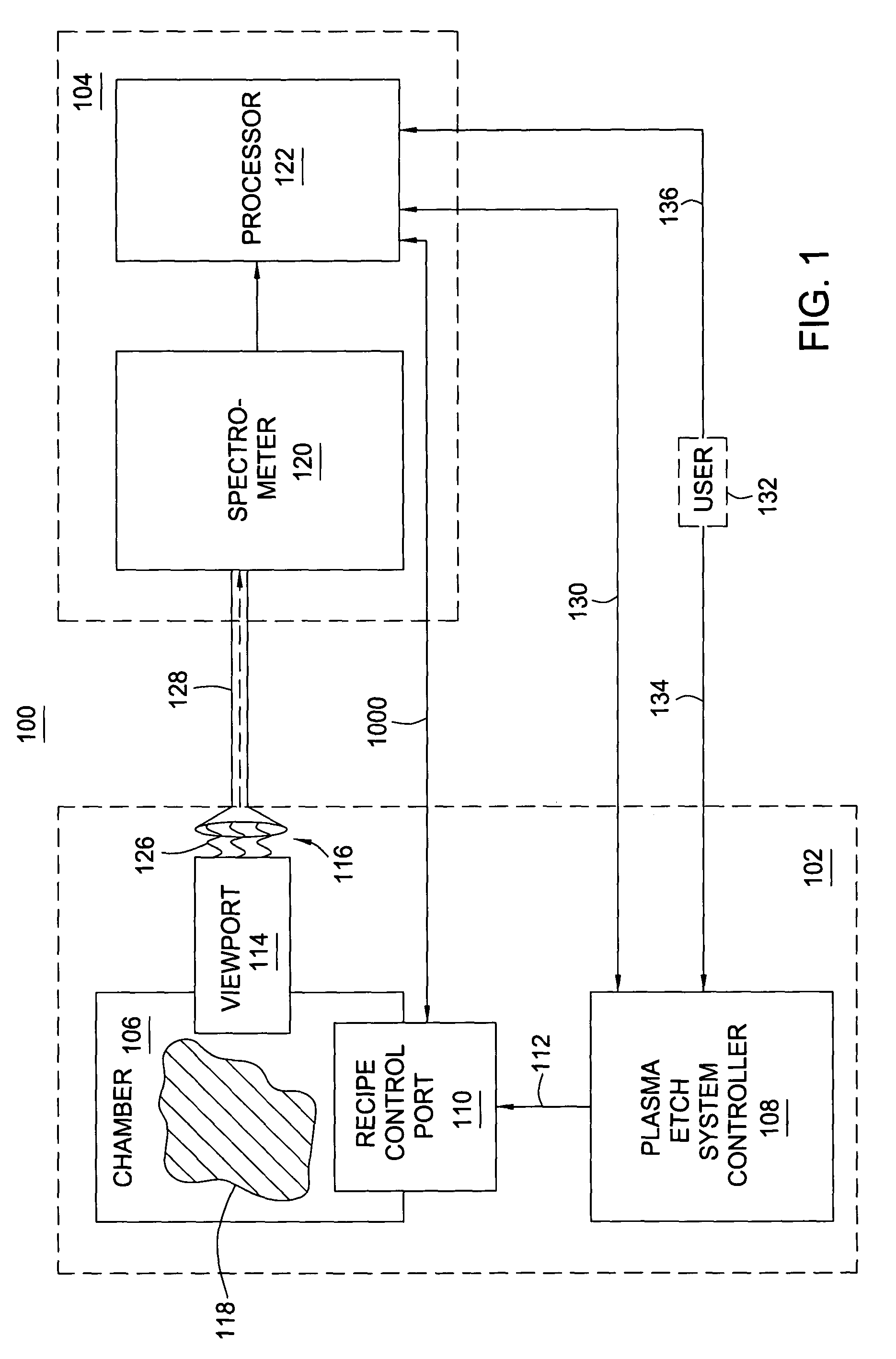
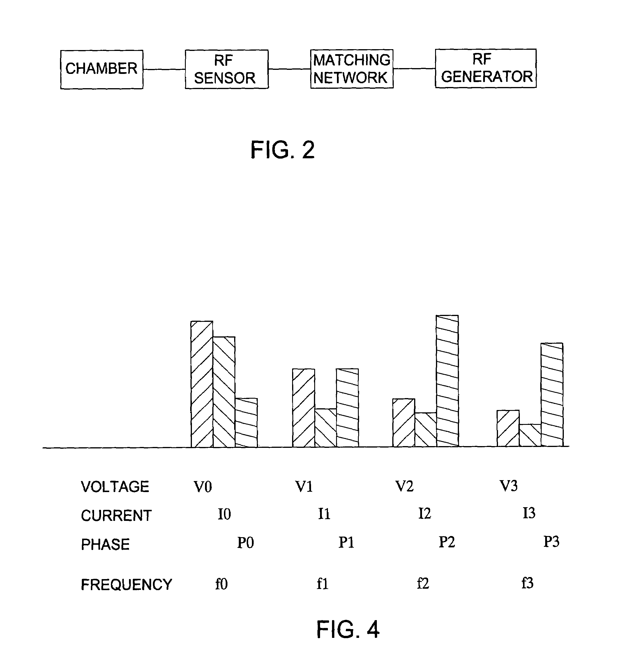
[0027]The invention involves measuring correlated attributes of a plasma process in a processing chamber, and by employing principal component analysis to analyze the correlated attributes; process state and chamber state information may be easily and accurately obtained for the process. For convenience, the present invention is described herein primarily with reference to plasma etch processes and plasma-based correlated attributes (e.g., plasma electromagnetic emissions state and RF state). Details of how plasma emission spectrum data can be collected and how principal component analysis can be used to identify principal components have been disclosed in commonly assigned U.S. Pat. No. 6,455,437, entitled “Method and Apparatus For Monitoring The Process State of A Semiconductor Device Fabrication Process, issued on Sep. 24, 2002, U.S. Pat. No. 6,413,867, entitled “Film Thickness Control Using Spectral Interferometry”, issued on Jul. 2, 2002, and U.S. Pat. No. 6,368,975, entitled “...


PUM

PropertyMeasurementUnit
optical wavelengthsaaaaaaaaaa
infrared wavelengthsaaaaaaaaaa
frequencyaaaaaaaaaa

Abstract

A method and apparatus for automatic determination of semiconductor plasma chamber matching a source of fault are provided. Correlated plasma attributes are measured for process used for calibration both in a chamber under study and in a reference chamber. Principal component analysis then is performed on the measured correlated attributes so as to generate steady principal components and transitional principal components; and these principal components are compared to reference principal components associated with a reference chamber. The process used for calibration includes a regular plasma process followed by a process perturbation of one process parameter. Similar process perturbation runs are conducted several times to include different perturbation parameters. By performing inner products of the principal components of chamber under study and the reference chamber, matching scores can be reached. Automatic chamber matching can be determined by comparing these scores with preset control limits. The potential source(s) of chamber fault can also be identified by the lowest matching score(s).

Description

BACKGROUND OF THE INVENTION[0001]1. Field of the Invention[0002]The present invention relates to semiconductor substrate processing systems. More particularly, the present invention relates to techniques and apparatus for automatically determining whether a substrate process chamber matches a reference substrate process chamber and the potential source(s) of chamber fault.[0003]2. Description of the Related Art[0004]Within the semiconductor industry, an ever present need exists for improved process repeatability and control. As new generations of integrated circuits employ smaller feature sizes than were contemplated in previous generations, greater demands are placed on the integrated circuit fabrication process. Deposition and etching one or more layers of a semiconductor substrate in a plasma environment are two of the most common steps in integrated circuit manufacturing. To ensure that a correct quantity and quality of film is deposited or etched, the plasma state of the proces...

Claims


Application Information

Patent Timeline
Patent Type & Authority Patents(United States)
IPC IPC(8): H01L21/00G01N21/73H01J37/32
CPCG01N21/73H01J37/32972H01J37/32935H01J37/32174
Inventor DAVIS, MATTHEW F.LIAN, LEI
Owner APPLIED MATERIALS INC
Why Eureka
Try Eureka