Methods and systems for controlling accumulation of electrical charge during semiconductor etching processes

a technology of electrical charge and etching process, which is applied in the direction of semiconductor/solid-state device testing/measurement, fluid pressure measurement, instruments, etc., can solve the problem of charge-induced damage occurring during plasma etching process, the most frequent type of damage, and the defect or damage in the wafer that occurs

Inactive Publication Date: 2009-06-04
AGERE SYST INC
View PDF4 Cites 3 Cited by
  • Summary
  • Abstract
  • Description
  • Claims
  • Application Information

AI Technical Summary

Benefits of technology

[0020]The invention provides a system and method for controlling the accumulation of electrical charges on a wafer located in a plasma etching chamber during a plasma etching process. The system comprises bias supply voltage control circuitry and bias power modulation circuitry. The bias supply voltage control circuitry is configured to provide a supply voltage that alternates at a selected frequency between a first supply voltage level and a second supply voltage level. The bias power modulation circuitry is configured to receive the alternating first and second supply voltage levels and to bias the plasma etching chamber at first and second bias voltage levels in response to receiving the first and second supply voltage levels, respectively.

Problems solved by technology

Therefore, any defect or damage in the wafer that occurs during the etching processes will have a much more significant impact on the total manufacturing process and product yield than a defect or damage in the wafer that occurs during other front-end processes, such as during implantation and various thermal processes.
Charge-induced damage occurring during plasma etching processes is the most frequent type of damage that occurs during the semiconductor manufacturing process.
When the electrical potential from these accumulated charges becomes sufficiently large, an uncontrolled discharge, i.e., arcing, will occur in the chamber.
A rapid uncontrolled discharge of the accumulated charges can cause damage to the wafer and / or to chamber parts.
Damage to the wafer can result in one or more of the semiconductor devices formed on the wafer being defective, and therefore unusable, which reduces yield.
Damage to the chamber can result in improper operations during the etch process that can lead to defects being formed in wafers during the etch process.
The aforementioned charge-induced damage can occur in any of these three steps.
Rapid discharge of accumulated charge, or arcing, will occur whenever the electric field associated with the accumulated charge is sufficiently greater than the dielectric strength of the material to cause dielectric breakdown to occur in the material, resulting in electrical paths being formed in the material.
The increase in the potential difference V4-V3 can result in an uncontrolled discharge of accumulated electrical charge, i.e., arcing, that can cause damage to the wafer.
This technique, however, typically results in a compromise in the etching profile and / or a sacrifice in etching efficiency.
By discharging the wafer prior to the plasma etching process, it is less likely that a sufficient amount of charge will accumulate during the plasma etching process to cause a rapid discharge to occur during the etching process.
This patent does not, however, provide a solution to the problem of discharge damages caused by the use of high plasma etching rates during the etching process.
Due to the large uncertainty of the charge buildup and distribution on the wafer caused by the antenna effect, it is extremely difficult to achieve a stable balance among, on one hand, controlling discharge, and on the other, maintaining an adequate etch profile and etch efficiency.
As a result, even with well-tuned plasma etching process configurations, semiconductor manufacturers commonly find that approximately 1% to 2% of wafers experience discharge damage.
With the ongoing trend of geometry sizes decreasing and pattern density increasing, the tolerance of semiconductor devices to charge buildup is becoming weaker.

Method used


Image

  • Methods and systems for controlling accumulation of electrical charge during semiconductor etching processes
  • Methods and systems for controlling accumulation of electrical charge during semiconductor etching processes
  • Methods and systems for controlling accumulation of electrical charge during semiconductor etching processes

Examples


Embodiment Construction

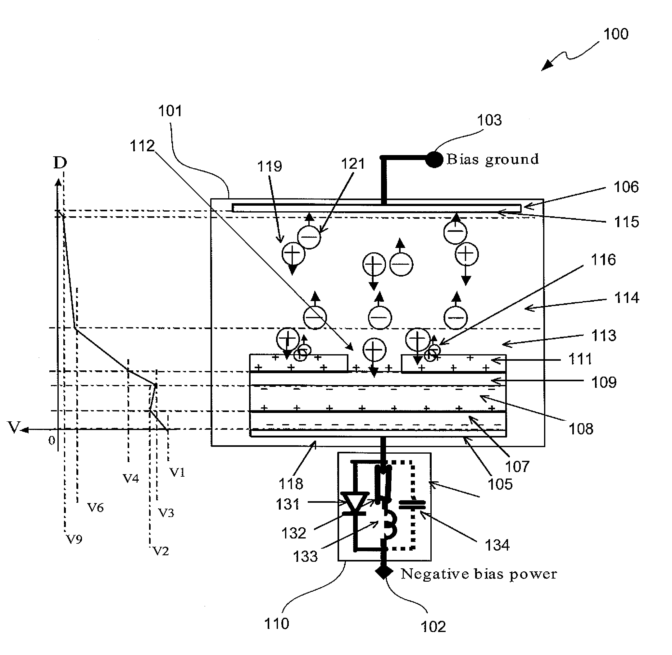
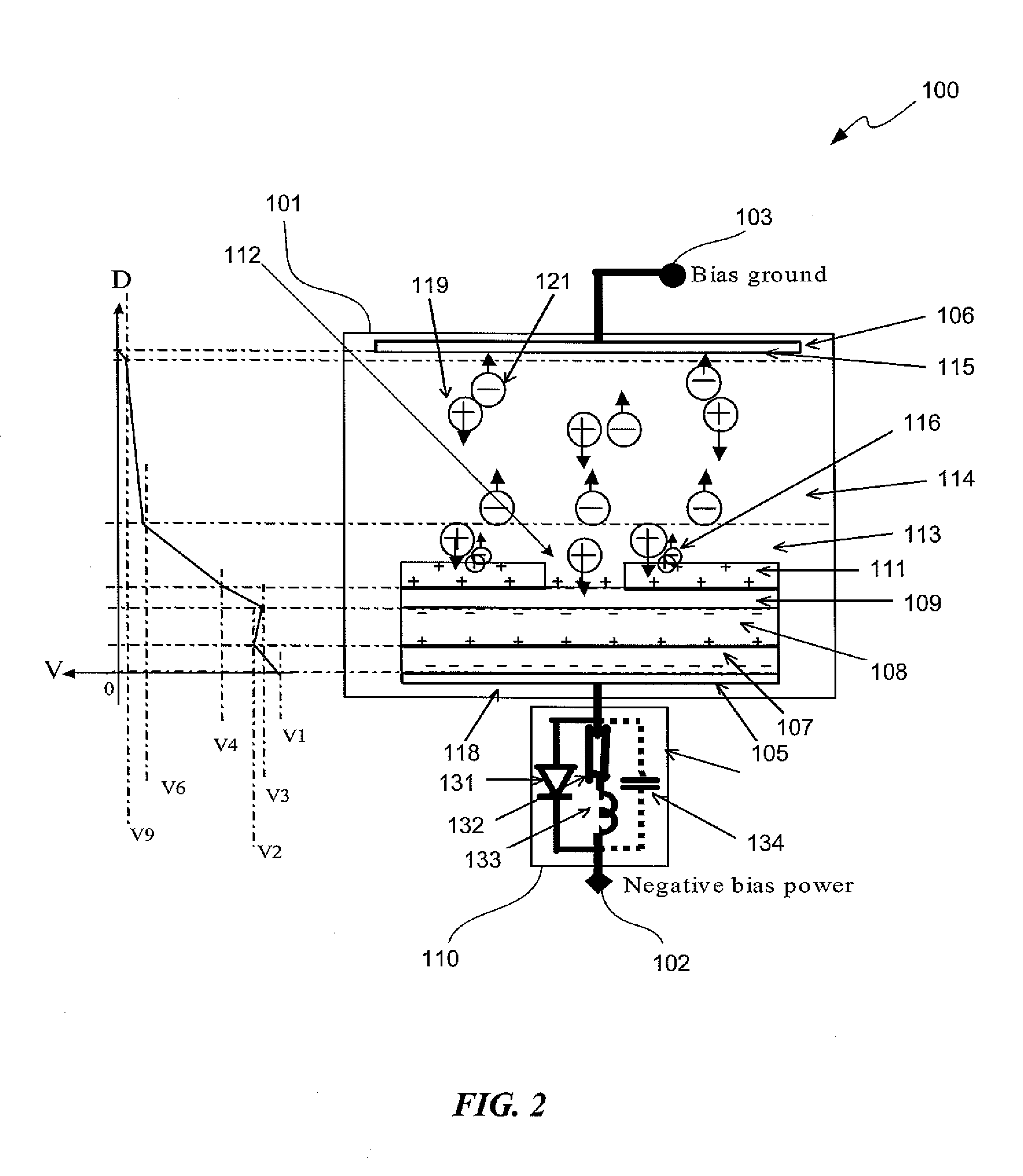
[0029]The invention provides a method and system for controlling the accumulation of electrical charge during a semiconductor plasma etching process performed in a plasma etching chamber. In accordance with the invention, the bias voltage supplied to the plasma etching chamber is modulated by a bias power modulation circuit to control the accumulation of electrical charge and to force the accumulated electrical charge to be periodically discharged at a controlled rate of discharge that prevents the wafer from being damaged. The manner in which this is accomplished in accordance with an illustrative embodiment will now be described with reference to FIGS. 2-5.

[0030]FIG. 2 illustrates a block diagram of a plasma etching system 100 equipped with a bias power modulation circuit 110 in accordance with an illustrative embodiment of the invention. The system 100 includes a chamber 101 that has a negative bias power terminal 102 and a bias ground terminal 103 electrically coupled to it. Ref...


PUM

PropertyMeasurementUnit
voltageaaaaaaaaaa
electrical chargeaaaaaaaaaa
frequencyaaaaaaaaaa

Abstract

A method and system are provided for controlling the accumulation of electrical charge during a semiconductor plasma etching process performed in a plasma etching chamber. The bias voltage supplied to the plasma etching chamber is modulated by a bias power modulation circuit to control the accumulation of electrical charge and to force the accumulated electrical charge to be periodically discharged at a controlled rate of discharge that prevents the wafer from being damaged.

Description

TECHNICAL FIELD OF THE INVENTION[0001]The invention relates to semiconductor fabrication processes. More particularly, the invention relates to controlling the buildup of electrical charge during etching processes that can result in damage to the semiconductor device and to the equipment used to perform the etching process.BACKGROUND OF THE INVENTION[0002]Plasma etching processes are widely used in the manufacturing of semiconductor devices to form patterns or structures in the semiconductor devices. Semiconductor devices are used in a wide variety of consumer products, including, for example, television sets, radios, computers, as well as in other types of equipment and products, such as biochips used for modern medical laboratory tests and optical components such as light gratings and multiplexers used in the communications industry.[0003]In order to improve the performance of products and equipment that incorporate semiconductor devices and to reduce their costs, the geometries o...

Claims


Application Information

Patent Timeline
Patent Type & Authority Applications(United States)
IPC IPC(8): C23F1/00
CPCH01J37/32706H01L22/14H01J37/32935
Inventor WANG, EDWARD AIGUOROSSI, NACE
Owner AGERE SYST INC
Why Eureka
Try Eureka