Semiconductor integrated circuit device and method of producing the same

a technology of integrated circuits and semiconductors, applied in the direction of cad circuit design, computer aided design, instruments, etc., can solve the problems of increasing development cost and development period of lsi, and achieve the effect of shortening the development period and reducing the development cos

Inactive Publication Date: 2007-01-30
PANASONIC CORP
View PDF32 Cites 26 Cited by
  • Summary
  • Abstract
  • Description
  • Claims
  • Application Information

AI Technical Summary

Benefits of technology

[0011]It is an object of the present invention to provide a configuration of a semiconductor integrated circuit device and a method of producing the same that can shorten the development period and reduce the development cost when a gate array-type semiconductor integrated circuit device becomes large in scale.

Problems solved by technology

This causes the development cost and development period of an LSI to increase.
However, the configuration of the conventional gate array LSI and a production method thereof have the following problems.

Method used


Image

  • Semiconductor integrated circuit device and method of producing the same
  • Semiconductor integrated circuit device and method of producing the same
  • Semiconductor integrated circuit device and method of producing the same

Examples


embodiment 1

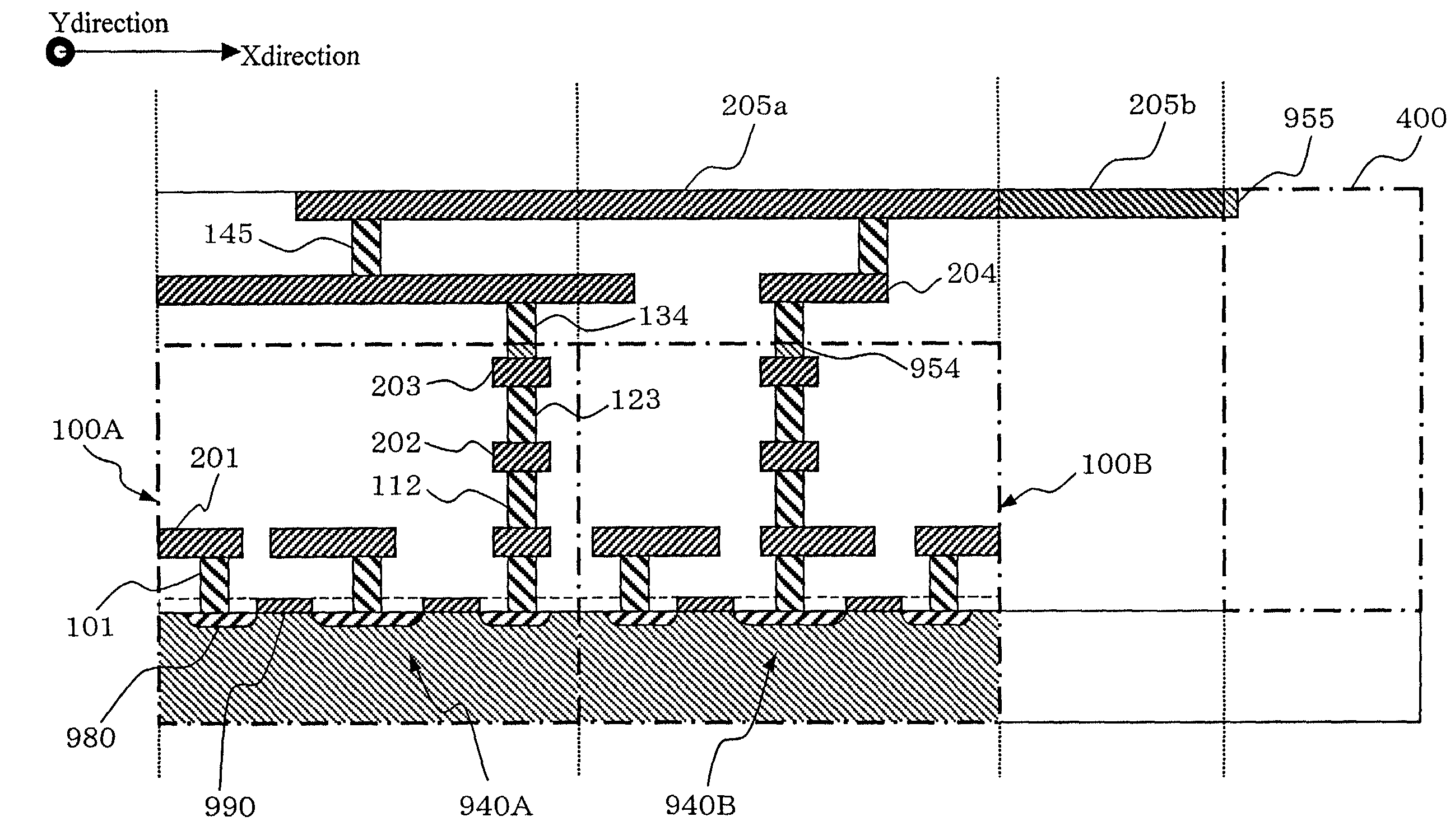
[0029]FIG. 1 is a sectional view showing a layout of an LSI of Embodiment 1. Logic cells 100A and 100B have a configuration in which second wiring layers 202 and third wiring layers 203 are added to the logic cells 900A and 900B in FIG. 9. First wiring layers 201 and second wiring layers 202, and the second wiring layers 202 and third wiring layers 203, are connected to each other through contact VIAs 112 and contact VIAs 123, respectively. Connecting pins 954 are formed at the top portions. The logic cells 100A and 100B are connected to each other through contact VIAs 134, fourth wiring layers 204, contact VIAs 145, and a fifth wiring layer 205a. The logic cell 100B is connected to a functional block 400 through a fifth wiring layer 205b and a connecting pin 955.

[0030]As described above, only three wiring layers are disposed in the conventional logic cell regions, whereas five wiring layers are disposed in the regions of the logic cells 100A and 100B, and the logic cells 100A and 1...

embodiment 2

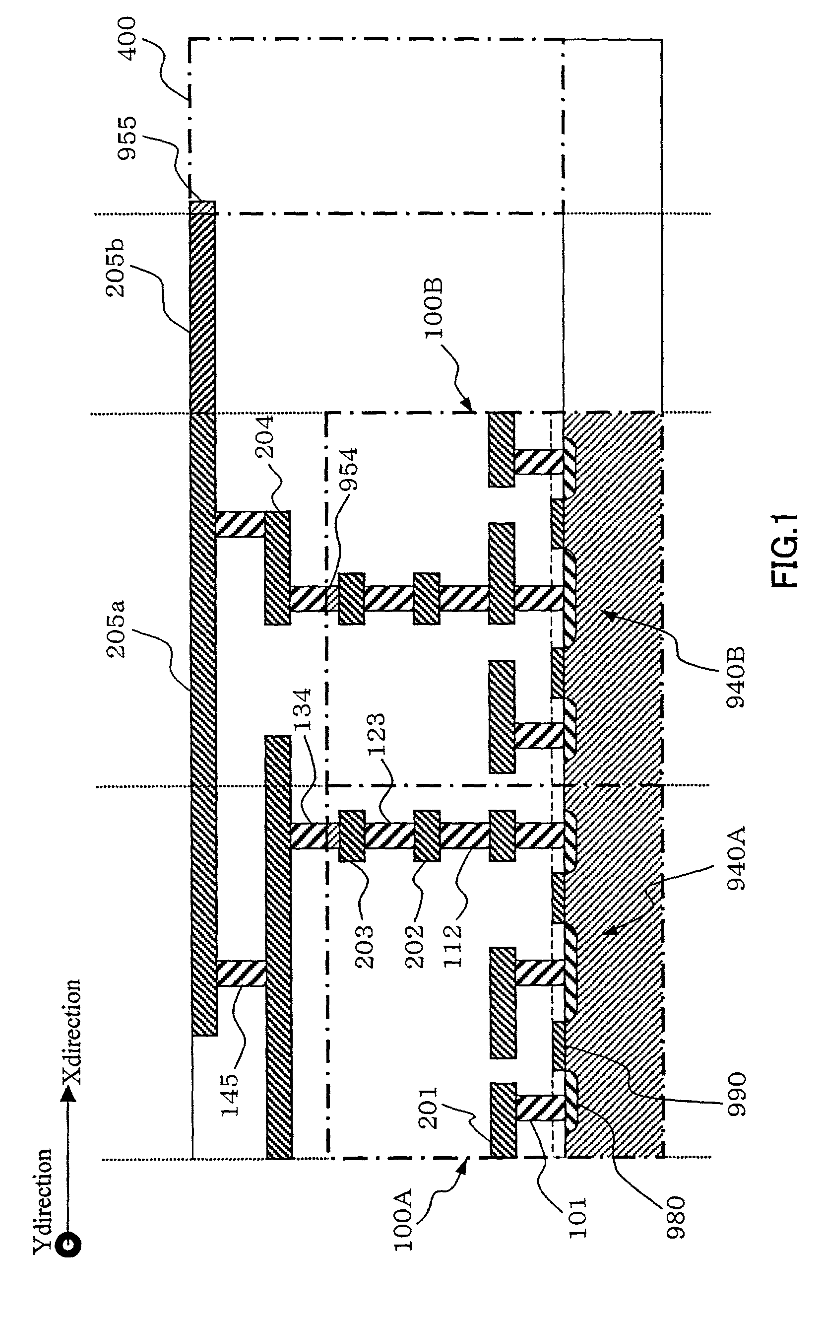
[0031]FIG. 2 is a structural view showing a layout of an LSI of Embodiment 2. In the present embodiment, in the regions of the logic cells 100A, 100B, and 100C, since five wiring layers are arranged, and connection cells 200A and 200B are inserted into lower two layers, upper three wiring layers can be corrected.

[0032]FIG. 3B shows a configuration of a connection cell 200 (200A or 200B in FIG. 2). The connection cell 200 is composed of contact VIAs 220 (101 or 112 in FIG. 2) and wiring patterns 230 (201A or 202B in FIG. 2) disposed immediately above the contact VIAs 220 and connected thereto. The contact VIAs 220 are disposed at positions corresponding to arbitrary grids 210 of base cells 940 (940A, 940B, or 940C in FIG. 2) as shown in FIG. 3A. In FIG. 3A, reference numeral 240 denotes a power supply line and reference numeral 250 denotes a ground line. FIG. 3C shows a stacked state of the base cell 940 in FIG. 3A and the connection cell 200 in FIG. 3B. The line A—A in FIG. 3C shows...

embodiment 3

[0034]FIG. 4 shows a layout of an LSI of Embodiment 3. In the present embodiment, a power supply cell 300 is inserted for the purpose of strengthening a power supply line in accordance with previously calculated power consumption of a logic block. Thus, it becomes possible to arrange up to five wiring layers while only the upper three wiring layers are allowed to be corrected.

[0035]FIG. 5B shows a configuration of the power supply cell 300. The power supply cell 300 is composed of the contact VIAs 112 and a wiring pattern 302 connected to the contact VIAs 112 and cells adjacent thereto. The contact VIAs 112 are disposed at positions corresponding to at least one grid 210 in the power supply line 240 in the base cell 940 shown in FIG. 5A. FIG. 5C shows a stacked state of the base cell 940 in FIG. 5A and the power supply cell 300 in FIG. 5B. The line B—B in FIG. 5C indicates a position of a cross section shown in FIG. 4.

[0036]A GND cell also can be constituted in the same way as in th...


PUM


Abstract

A semiconductor integrated circuit device has a plurality of CMOS-type base cells arranged on a semiconductor substrate and m wiring layers, and gate array type logic cells are composed of the base cells and the wiring layers. Wiring within and between the logic cells is constituted by using only upper n (n<m) wiring layers. It becomes possible to shorten a development period and reduce a development cost when a gate array type semiconductor integrated circuit device becomes large in scale.

Description

BACKGROUND OF THE INVENTION[0001]1. Field of the Invention[0002]The present invention generally relates to a semiconductor integrated circuit device and a method of producing the same. More particularly, the present invention relates to a configuration of logic cells of a CMOS-type gate array and a method of producing functional blocks by using the logic cells.[0003]2. Related Background Art[0004]In recent years, semiconductor integrated circuit devices (hereinafter, referred to as an “LSI”) have tended toward higher integration and higher performance along with a finer process. This causes the development cost and development period of an LSI to increase. Under such circumstances, an LSI including gate array cells is suitable for the shortening of a development period and the reduction in cost or the flexible production, and finds wide applications, because such a method of producing an LSI can be designed with only wiring patterns by using CAD or the like.[0005]Hereinafter, the co...

Claims


Application Information

Patent Timeline
Patent Type & Authority Patents(United States)
IPC IPC(8): H01L27/10H01L23/48H01L29/73H01L29/739H01L29/74G06F17/50H01L27/02H01L27/118
CPCG06F17/5068G06F17/5077H01L27/11807H01L27/118H01L27/0207Y10S257/905Y10S257/909G06F30/394G06F30/39
Inventor TOKUNAGA, SHINYAFURUYA, SHIGEKIHINATSU, YUUJI
Owner PANASONIC CORP
Why Eureka
Try Eureka