Electronic component and method for manufacturing the same

a technology of electronic components and manufacturing methods, applied in piezoelectric/electrostrictive devices, generators/motors, printing, etc., can solve the problems of attracting fluctuation, affecting the quality of components, so as to achieve a small surface area

Inactive Publication Date: 2007-01-30
PANASONIC CORP
View PDF20 Cites 116 Cited by
  • Summary
  • Abstract
  • Description
  • Claims
  • Application Information

AI Technical Summary

Benefits of technology

[0008]An electronic component according to the present invention includes a substrate; a piezoelectric material layer supported directly or indirectly by the substrate; a first electrode arranged on a surface of the piezoelectric material layer on an opposite side of the substrate; and a second electrode arranged on a surface of the piezoelectric material layer on the substrate side. The piezoelectric material layer is sandwiched between the first electrode and the second electrode. The first electrode has a smaller surface area than the piezoelectric material layer. A portion where the piezoelectric material layer is exposed from the first electrode includes a portion that is thinner than a thickness of the piezoelectric material layer between the first electrode and the second electrode.

Problems solved by technology

Accordingly, the precision of the thickness of the piezoelectric material corresponds to the precision of the component's frequency, and thus thickness adjustments are an important issue.
Furthermore, this creates the problem of inviting fluctuation in parameters such as the electromechanical coupling coefficient.
Furthermore, the problem also arises that a modified layer occurs in a portion of the surface electrode 207 due to etching and the resistance is similarly raised, thus worsening the Q value.
Furthermore, empirically, the problem also arises that spurious signals, which are unwanted oscillations, tend to be produced when performing etching on portions of excitation portions of electrodes.
With the method according to JP 2002-335141A, a process by which a surface loading layer 211 is arranged becomes necessary, thus leading to increased costs.
Since the surface loading layer 211 is arranged on a surface layer electrode 210, which is an excitation electrode, the problem arises in that it becomes easier for spurious signals to be produced.

Method used


Image

  • Electronic component and method for manufacturing the same
  • Electronic component and method for manufacturing the same
  • Electronic component and method for manufacturing the same

Examples


embodiment 1

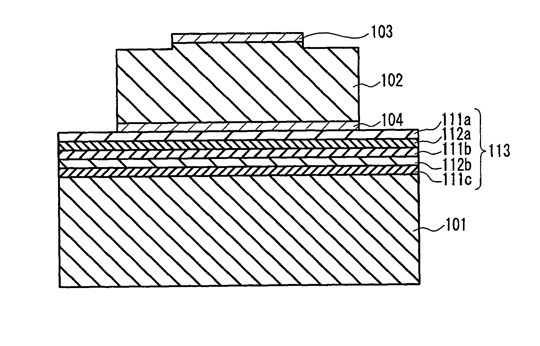
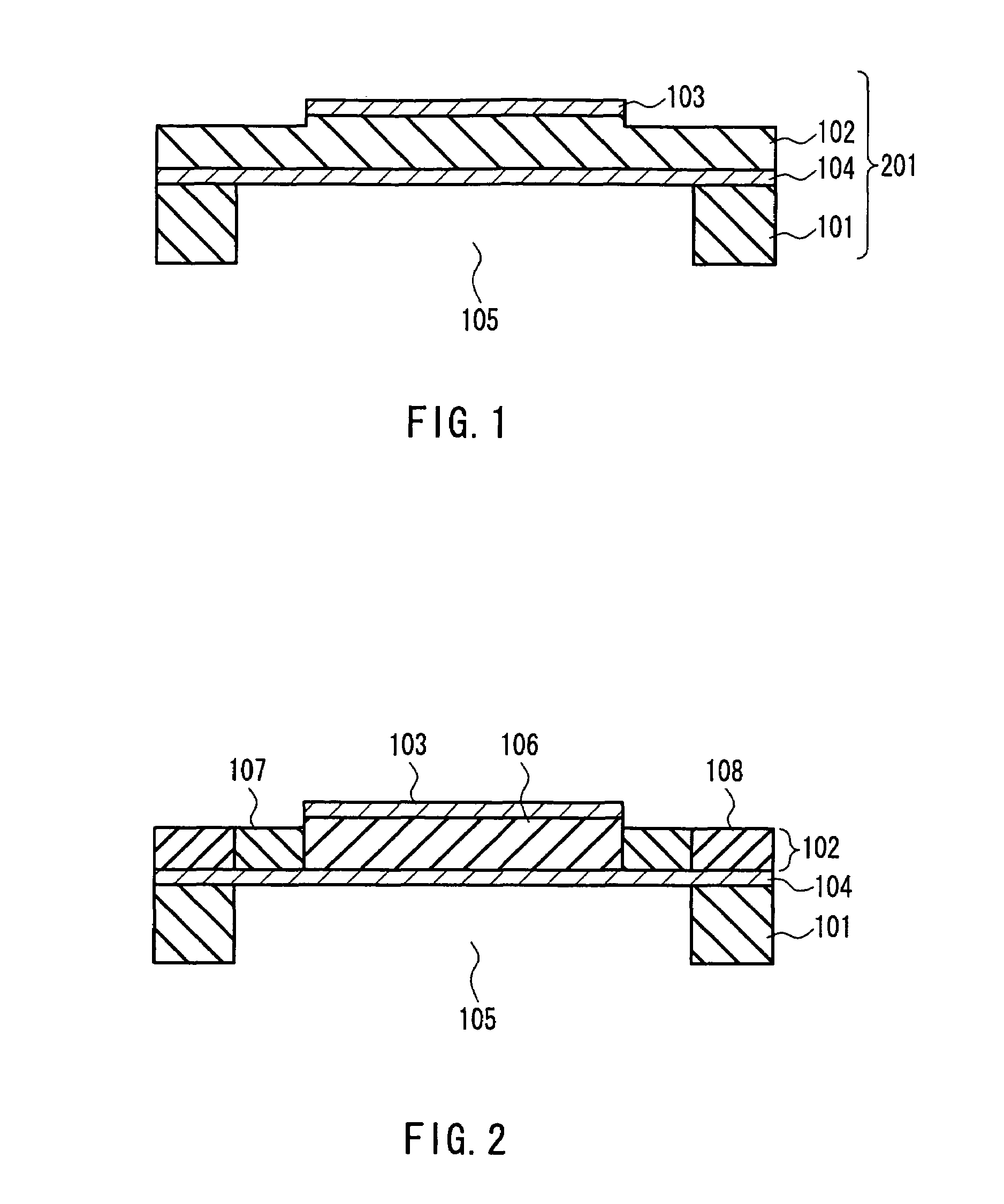
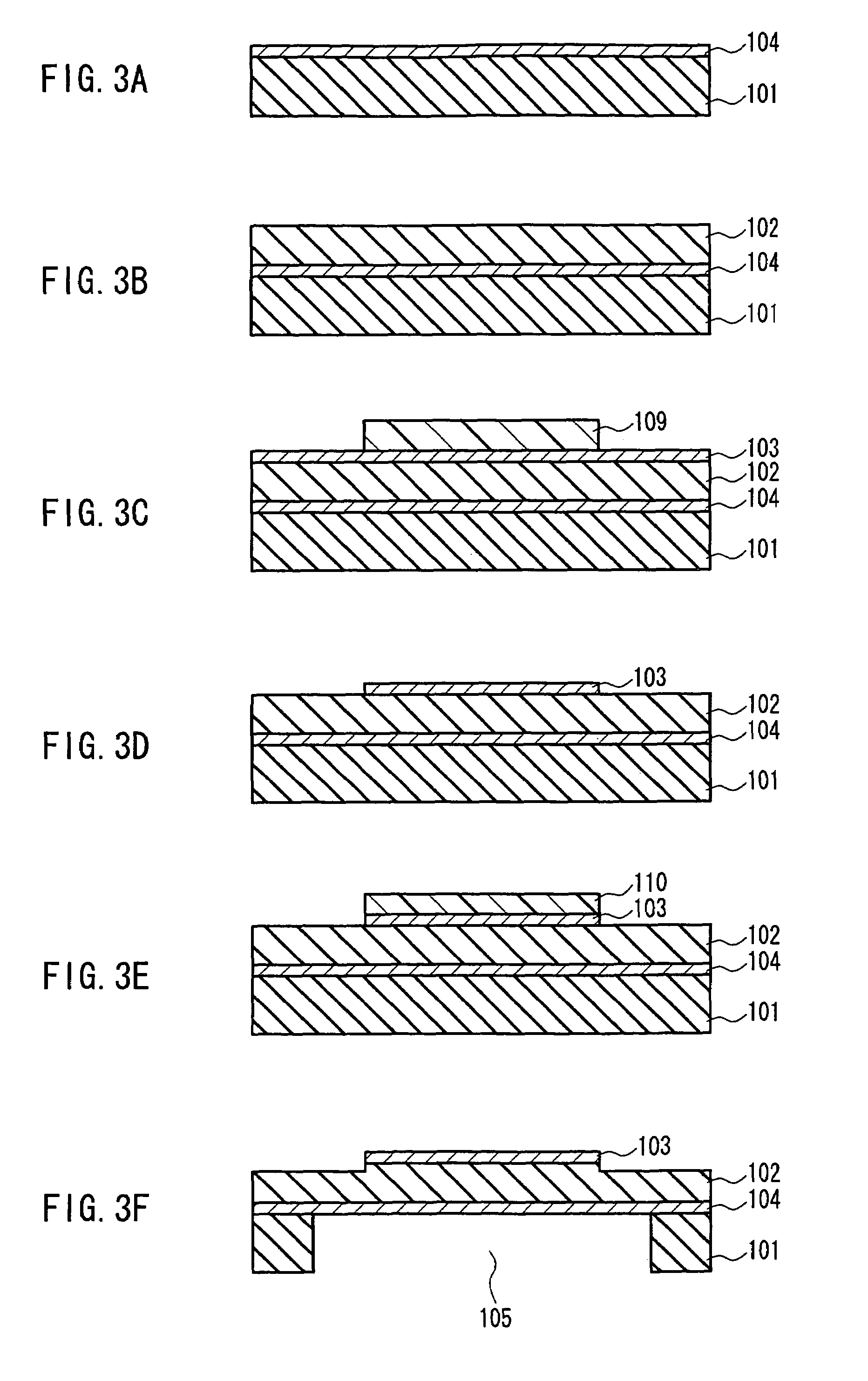
[0072]A first embodiment of the present invention is described using FIGS. 1 and 2 and 3A to 3F. FIGS. 1 and 2 are cross sections of a resonator portion of an electronic component according to the present embodiment. The electronic component may be configured by a single resonator as shown in these drawings, or a collection of a plurality of resonators. FIGS. 3A to 3F show a method for manufacturing an electronic component.

[0073]First, the configuration of the present embodiment is described. Reference numeral 101 denotes a substrate, for example, a silicon substrate. Reference numeral 102 denotes a piezoelectric material layer, for example, a thin film of aluminum nitride. Reference numeral 103 denotes a first electrode for excitation, which applies an electrical field to the piezoelectric material layer 102 to achieve elastic oscillation. Reference numeral 104 denotes a second electrode that is arranged in a position opposite the first electrode 103. For example, in the present em...

embodiment 2

[0085]A second embodiment of the present invention is described using FIGS. 4 to 6A–6B. FIGS. 4 and 5 are cross sections of a resonator portion of an electronic component according to the present embodiment. The electronic component may be configured with a single resonator as shown in these drawings, or a collection of a plurality of resonators. FIGS. 6A and 6B show part of a method for manufacturing an electronic component. Common reference numerals are the same as in the first embodiment. The present embodiment is configured such that a thickness of only a portion of the second piezoelectric material area 107 is smaller than the thickness of the first piezoelectric material area 106. Furthermore, since except for the fourth step the manufacturing method here is overall the same as in the first embodiment, only the fourth step and the masking step prior to it will be described here. As shown in FIG. 6A, patterning is carried out such that the masking material 110 is provided with ...

embodiment 3

[0086]A manufacturing method of a third embodiment of the present invention is described using FIGS. 3 and 12. At the stage of the first step in the present embodiment, the substrate 101 is a 4-inch wafer silicon substrate. The first and second steps described in the first embodiment (FIGS. 3A and 3B) are carried out. After this, film thickness measurements are performed using an ellipsometer on 16 locations on the wafer as shown in FIG. 12. The results are shown in Table 1.

[0087]

TABLE 1Position in wafer12345678Difference from−0.962−1.442−1.442−1.442−0.481−0.962−1.442−1.923predeterminedvalue (%)CategoryCDDDBCDEPosition in wafter910111213141516Difference from0−0.962−1.442−1.9230−0.481−1.442−1.923predeterminedvalue (%)CategoryACDEABDE

[0088]The numbers for positions in the wafer correspond to the positions shown in FIG. 12. The difference from the predetermined value refers to the discrepancy rate (%) of the measured thickness from the predetermined thickness. Furthermore, category ref...


PUM

PropertyMeasurementUnit
thicknessaaaaaaaaaa
thicknessaaaaaaaaaa
thicknessaaaaaaaaaa

Abstract

An electronic component includes a substrate; a piezoelectric material layer supported directly or indirectly by the substrate; a first electrode arranged on a surface of the piezoelectric material layer on an opposite side of the substrate; and a second electrode arranged on a surface of the piezoelectric material layer on the substrate side. The piezoelectric material layer is sandwiched between the first electrode and the second electrode. The first electrode has a smaller surface area than the piezoelectric material layer. A portion where the piezoelectric material layer is exposed from the first electrode includes a portion that is thinner than a thickness of the piezoelectric material layer between the first electrode and the second electrode. Thus, it is possible to configure a resonator with a higher frequency than its ordinary resonance, and it is easy to achieve an adjustment of the resonance frequency of the resonator, as well as improving the yield of the component and enabling the configuration of an electronic component that includes a plurality of resonators of different frequencies.

Description

FIELD OF THE INVENTION[0001]The present invention relates to electronic components and methods for manufacturing the same that are useful in the predetermined frequency bands of filters and oscillators for example. More specifically, the present invention relates to electronic components and methods for manufacturing the same that are used as a frequency filter (hereafter “filter”) or an oscillator mounted in a communication device such as a mobile telephone or keyless entry device and the like.BACKGROUND OF THE INVENTION[0002]Along with advances toward higher frequencies and miniaturization of information and telecommunications devices such as portable telephones, electronic components such as filters and oscillators used in these devices are also undergoing advances toward higher frequencies and miniaturization. As shown in FIG. 11 for example, filters and the like are being used in which a bulk acoustic wave (BAW) resonator is used. Ordinarily, piezoelectric materials are used to...

Claims


Application Information

Patent Timeline
Patent Type & Authority Patents(United States)
IPC IPC(8): H01L41/08H03H3/04H03H9/17H03H9/56
CPCH03H3/04H03H9/173H03H9/174H03H9/175H03H9/564B41J2002/14266Y10T29/49128H03H2003/0478Y10T29/4913Y10T29/49005Y10T29/49135Y10T29/42H03H2003/0435
Inventor NAMBA, AKIHIKOONISHI, KEIJITAKEDA, KATSU
Owner PANASONIC CORP
Why Eureka
Try Eureka