Ultra thin, single phase, diffusion barrier for metal conductors
a diffusion barrier and metal conductor technology, applied in the field of interconnect semiconductor structures, can solve the problems of a large number of undesirable properties, a large amount of cu, and a general diffusion through the dielectric material
- Summary
- Abstract
- Description
- Claims
- Application Information
AI Technical Summary
Benefits of technology
Problems solved by technology
Method used
Image
Examples
example
[0065]A series of experiments were performed in order to demonstrate the effectiveness of the alpha-W barrier layer of the present invention.
I. Demonstration of Impermeability
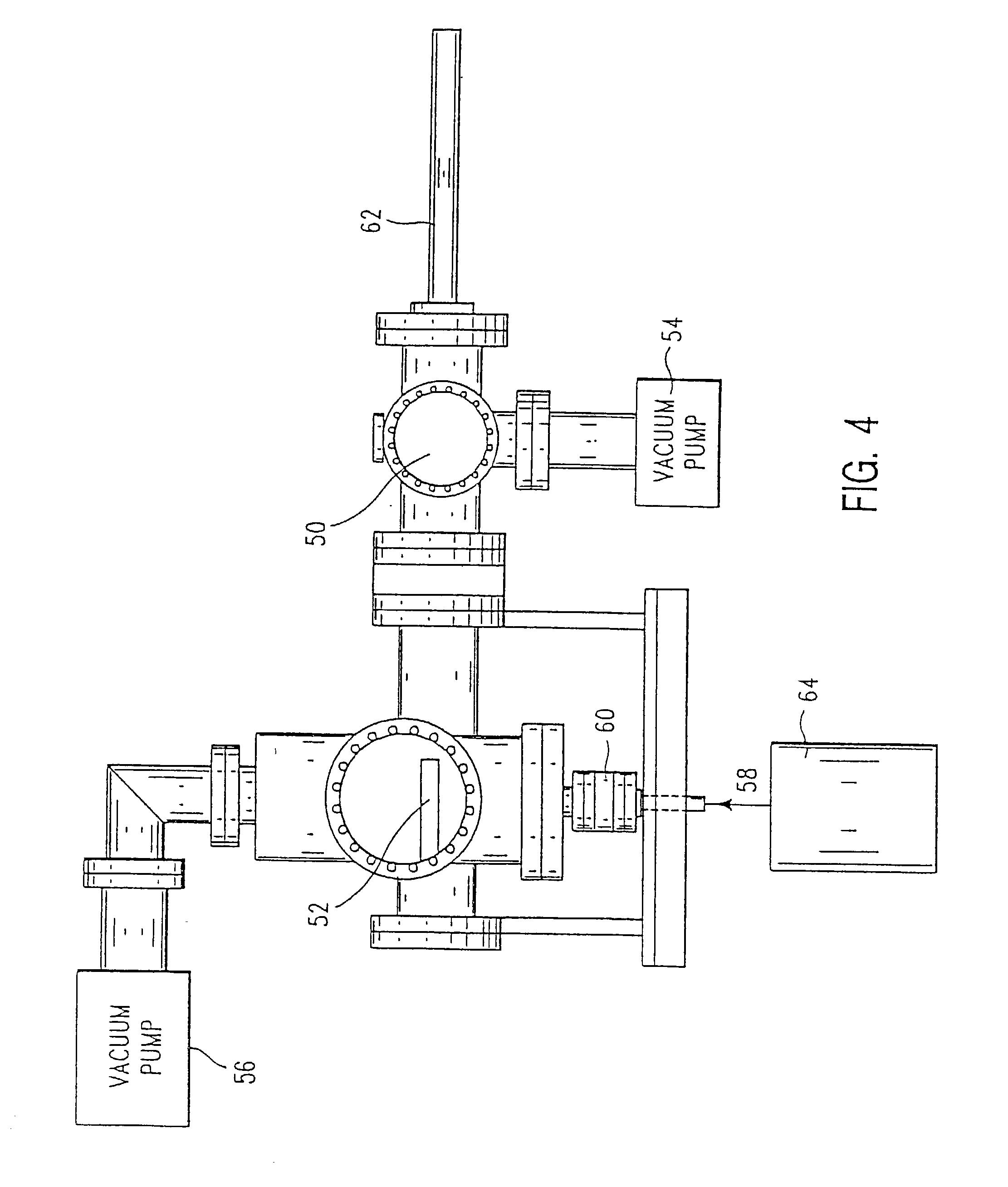
[0066]A substrate comprising a planar layer of Cu having a thickness of 300 nm formed on the surface of silicon was exposed to W(CO)6 in accordance with the CVD processing conditions mentioned hereinabove. Specifically, the W deposition was carried out in a CVD apparatus at a temperature of about 450° C. and a deposition pressure of about 5×10⁴ Torr. Deposition was carried out at these conditions for a time period of about 8 minutes which was sufficient to form a continuous alpha-W barrier layer having a thickness of about 7 nm.
[0067]The resulting structure was analyzed by X-ray photoemission spectroscopy (XPS) to ensure that there was no Cu present on the surface. This sample which contained no Cu on the surface was then annealed in vacuum for 70 hours at 500° C. These test conditions were more stringent than ...
PUM
 Abstract
Description
Claims
Application Information


