Memory circuit, display circuit, and display device

Inactive Publication Date: 2007-02-06
ADVANCED LCD TECH DEVMENT CENT
View PDF14 Cites 11 Cited by
  • Summary
  • Abstract
  • Description
  • Claims
  • Application Information

AI Technical Summary

Benefits of technology

[0017]With the memory circuit, display circuit, and display device, when the source and drain of the transistor are connected to the first and second storage capacitances, the charges in the first and second storage capacitances are redistributed to provide the data signal as the analog drive voltages of the positive and negative polarities. These analog drive voltages are continuously held by the first and second storage capacitances while the data signal does not need to

Problems solved by technology

Such frequent transfer of the data signal makes it difficult to keep power dissipation low.
Thus, intermediate gradations cannot be obtained for displaying a full-color image.
It is difficult to realize the configurations (1) and (2) in a small pixel size.
With the configuration (3), many pr

Method used


Image

  • Memory circuit, display circuit, and display device
  • Memory circuit, display circuit, and display device
  • Memory circuit, display circuit, and display device

Examples


Example

[0028]A liquid crystal display device according to an embodiment of the present invention will now be described with reference to the accompanying drawings.

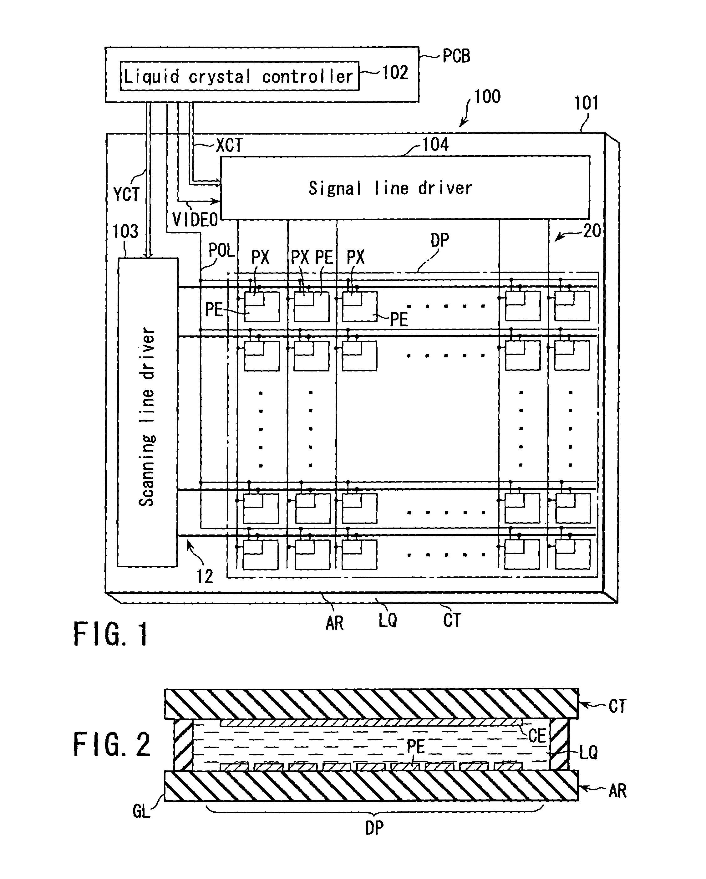
[0029]FIG. 1 shows a schematic circuit configuration of the liquid crystal display device 100, and FIG. 2 shows a schematic sectional structure of the liquid crystal display device 100.

[0030]The liquid crystal display device 100 includes a liquid crystal display panel 101 and a liquid crystal controller 102 for controlling the liquid crystal display panel 101. The liquid crystal display panel 101 has a structure that a liquid crystal layer LQ is held between an array substrate AR and a counter substrate CT. The liquid crystal controller 102 is disposed on a drive circuit board PCB provided independently of the liquid crystal display panel 101.

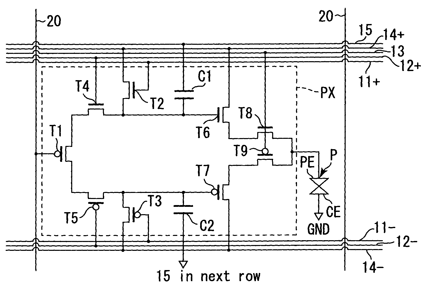
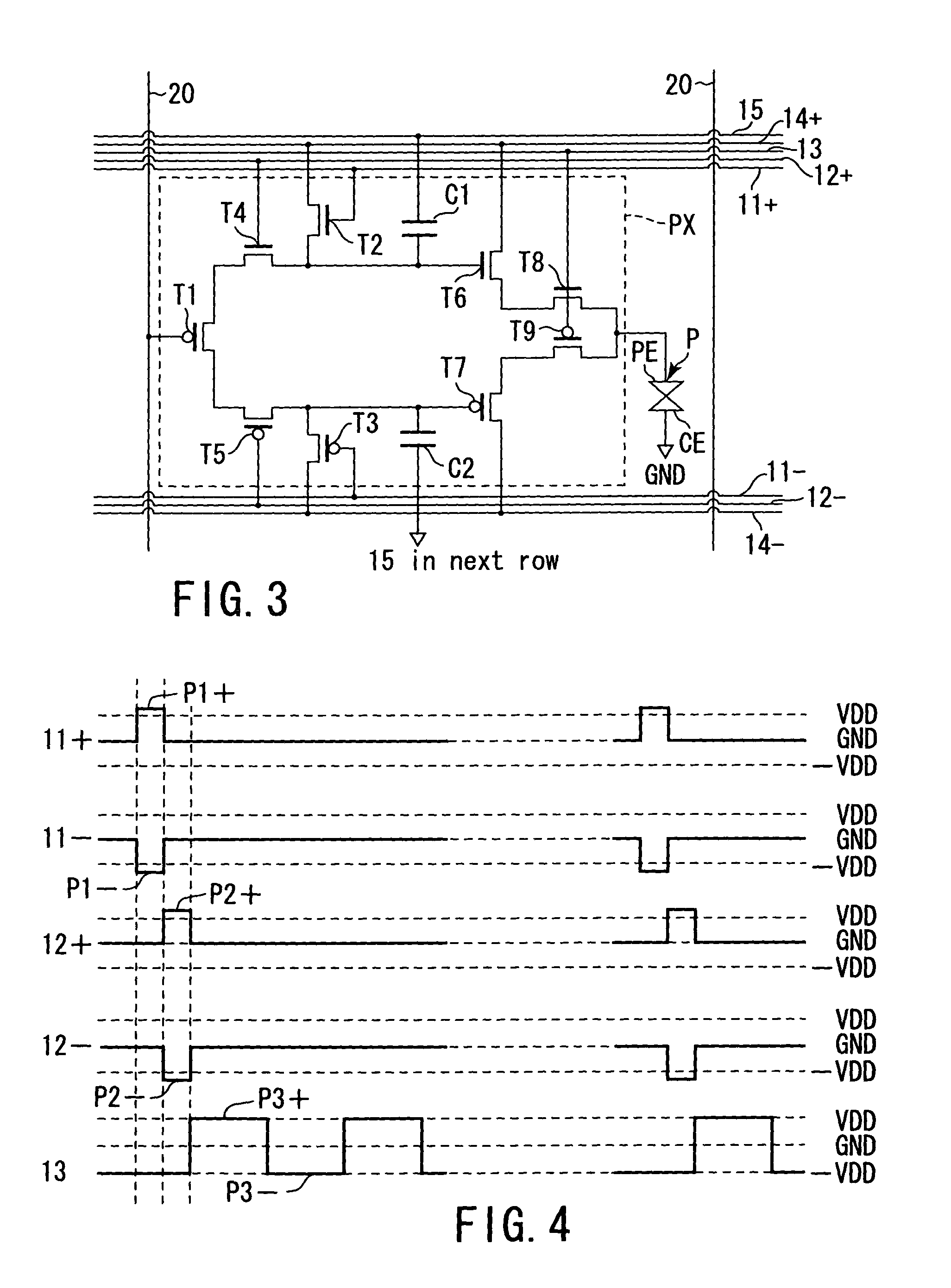
[0031]The array substrate AR includes a plurality of pixel electrodes PE arrayed in a matrix of rows and columns within a display area DP on a glass plate GL, a plurality of scanning lines 1...


PUM


Abstract

A liquid crystal display includes pixels arrayed in a matrix of rows and columns, scanning lines extending along the rows of the pixels, signal lines extending along the columns of the pixels, and pixel driving sections which are disposed near intersections of the scanning lines and signal lines, and each of which is controlled via one scanning line to capture a data signal on one signal line and output the data signal to one pixel. Particularly, each pixel driving section includes a memory circuit having a transistor whose gate is connected to the one signal line, and first and second storage capacitances which are charged to positive and negative power supply voltages and connected to a source and drain of the transistor to store the data signal as analog drive voltages of positive and negative polarities, respectively.

Description

CROSS-REFERENCE TO RELATED APPLICATIONS[0001]This application is based upon and claims the benefit of priority from the prior Japanese Patent Application No. 2002-270665, filed Sep. 17, 2002, the entire contents of which are incorporated herein by reference.BACKGROUND OF THE INVENTION[0002]1. Field of the Invention[0003]The present invention generally relates to a display device, such as a liquid crystal display device or EL (Electro Luminescence) display device, and more particularly to a memory circuit, display circuit, and display device arranged to store a data signal for a pixel, for example.[0004]2. Description of the Related Art[0005]In the liquid crystal display device, a large number of pixels are arrayed in a matrix of rows and columns so as to display an image corresponding to one frame of a video signal input from an external signal source such as a personal computer. The video signal is serial-parallel converted into data signals to be applied as analog drive voltages t...

Claims


Application Information

Patent Timeline
IPC IPC(8): G09G3/36G02F1/133
CPCG09G3/3648G09G3/3614G09G2300/0842G09G2300/0809G02F1/133
Inventor MATSUMURA, MASAKIYOKORENARI, TAKAHIRO
Owner ADVANCED LCD TECH DEVMENT CENT
Why Eureka
Try Eureka