Semiconductor device having deep trench charge compensation regions and method

a technology of charge compensation and semiconductors, applied in the direction of semiconductor devices, basic electric elements, electrical appliances, etc., can solve the problems of increased burden on peripheral control circuits, increased cost of rdson, and significant manufacturing challenges

Active Publication Date: 2007-02-13
SEMICON COMPONENTS IND LLC
View PDF21 Cites 95 Cited by
  • Summary
  • Abstract
  • Description
  • Claims
  • Application Information

AI Technical Summary

Benefits of technology

[0019]In addition, the device of the present invention may embody either a cellular design (where the body regions are a plurality of cellular regions) or a single body design (where the body region is compromised of a single region formed in an elongated pattern, typically in a serpentine pattern). However, the device of the present invention will be described as a cellular design throughout the description for ease of understanding. It should be understood that it is intended that the present invention encompass both a cellular design and a single base design.

Problems solved by technology

However, this is often at the expense of Rdson.
This trade-off in performance is a major design challenge for manufacturers and users of high voltage power switching devices.
Although superjunction devices look promising, significant challenges still exist in manufacturing them.
Another problem with present high voltage power switch products is that they typically require a large input (e.g., gate or control electrode) charge for switching from one state to another.
This requirement places, among other things, an extra burden on peripheral control circuitry.

Method used


Image

  • Semiconductor device having deep trench charge compensation regions and method
  • Semiconductor device having deep trench charge compensation regions and method
  • Semiconductor device having deep trench charge compensation regions and method

Examples


Embodiment Construction

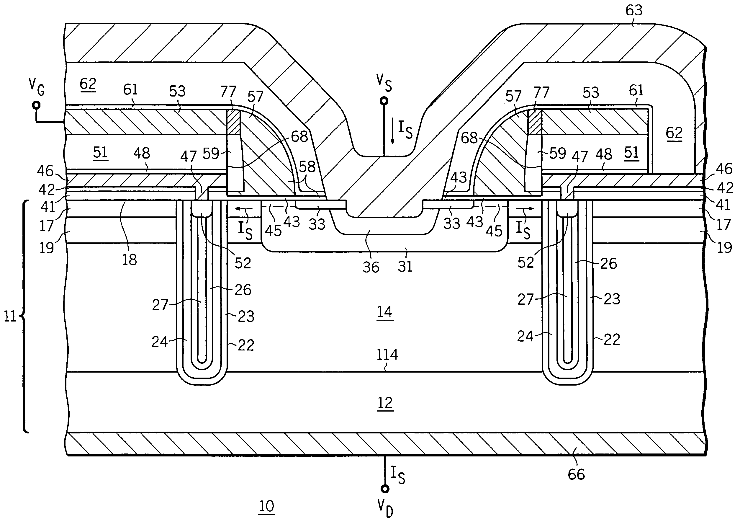
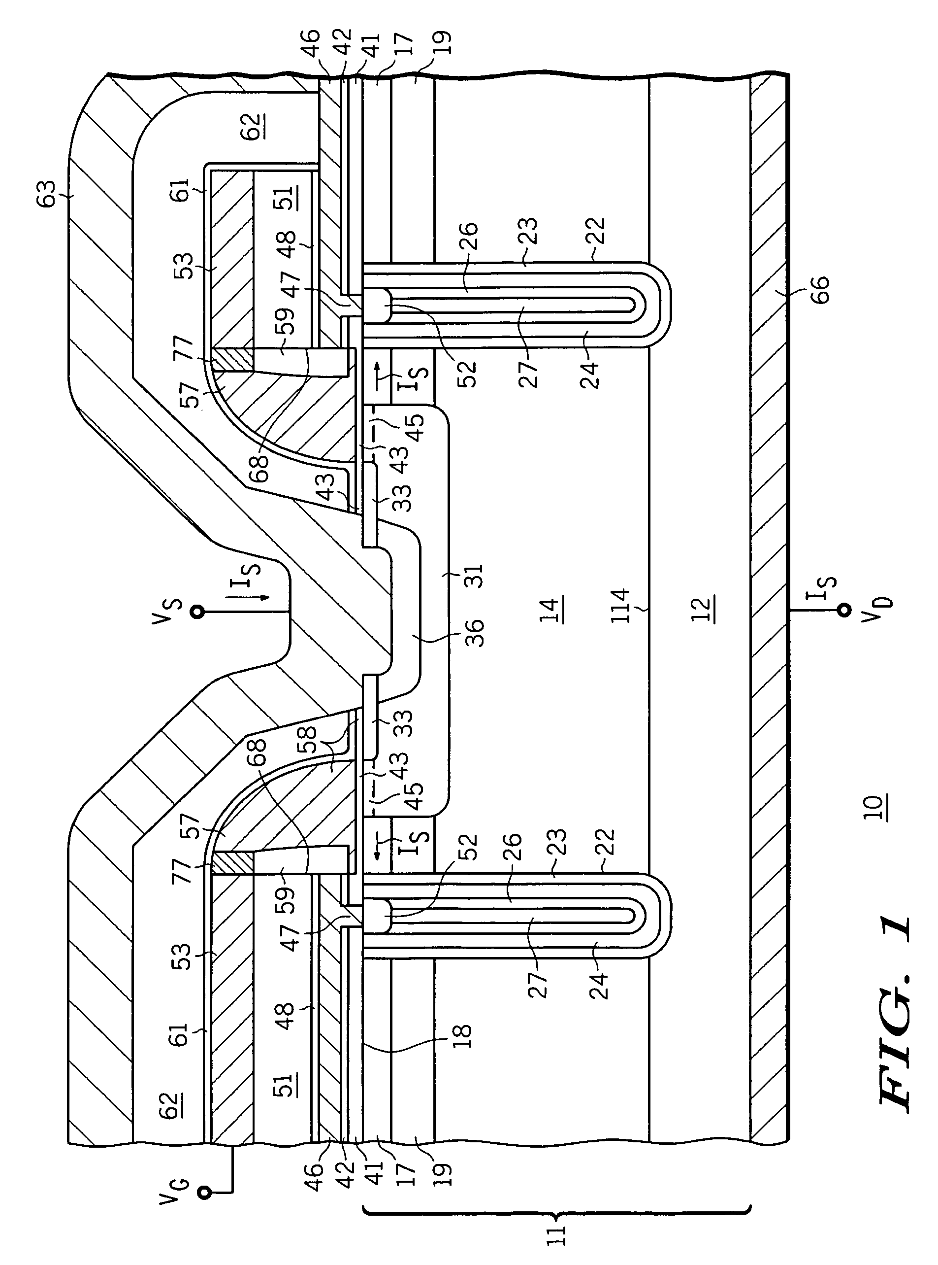
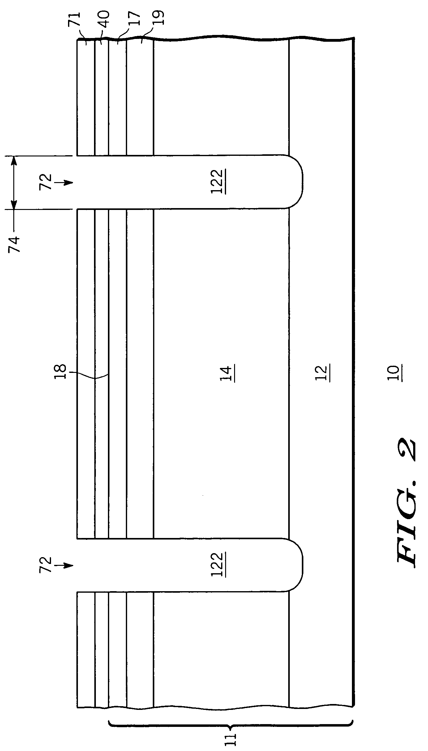
[0018]For ease of understanding, elements in the drawing figures are not necessarily drawn to scale, and like element numbers are used where appropriate throughout the various figures. While the discussion below describes an n-channel device, the invention also pertains to p-channel devices, which may be formed by reversing the conductivity type of the described layers and regions.

[0019]In addition, the device of the present invention may embody either a cellular design (where the body regions are a plurality of cellular regions) or a single body design (where the body region is compromised of a single region formed in an elongated pattern, typically in a serpentine pattern). However, the device of the present invention will be described as a cellular design throughout the description for ease of understanding. It should be understood that it is intended that the present invention encompass both a cellular design and a single base design.

[0020]FIG. 1 shows an enlarged partial cross-...


PUM


Abstract

In one embodiment, a semiconductor device is formed in a body of semiconductor material. The semiconductor device includes a charge compensating trench formed in proximity to active portions of the device. The charge compensating trench includes a trench filled with various layers of semiconductor material including opposite conductivity type layers.

Description

BACKGROUND OF THE INVENTION[0001]This invention relates generally to semiconductor devices, and more specifically to power switching devices and methods of their manufacture.[0002]Metal-oxide semiconductor field effect transistors (MOSFETs) are a common type of power switching device. A MOSFET device includes a source region, a drain region, a channel region extending between the source and drain regions, and a gate structure provided adjacent to the channel region. The gate structure includes a conductive gate electrode layer disposed adjacent to and separated from the channel region by a thin dielectric layer.[0003]When a MOSFET device is in the on state, a voltage is applied to the gate structure to form a conduction channel region between the source and drain regions, which allows current to flow through the device. In the off state, any voltage applied to the gate structure is sufficiently low so that a conduction channel does not form, and thus current flow does not occur. Dur...

Claims


Application Information

Patent Timeline
Patent Type & Authority Patents(United States)
IPC IPC(8): H01L29/94
CPCH01L21/761H01L29/0634H01L29/0646H01L29/7811H01L29/66719H01L29/66727H01L29/0638H01L29/0661H01L29/0696H01L29/1095H01L29/402H01L29/41766H01L29/42376H01L29/0878
Inventor LOECHELT, GARY H.ZDEBEL, PETER J.GRIVNA, GORDON M.
Owner SEMICON COMPONENTS IND LLC
Why Eureka
Try Eureka