Supercharge Your Innovation With Domain-Expert AI Agents!

Resin molding die and production method for semiconductor devices using the same

Inactive Publication Date: 2007-02-20
SHARP KK
View PDF26 Cites 0 Cited by
  • Summary
  • Abstract
  • Description
  • Claims
  • Application Information

AI Technical Summary

Benefits of technology

[0018]In still another embodiment of the invention, the air vent has an interspace of such dimensions that the resin being filled in the cavity expels air to the air vent, and that the resin cures within the air vent without leaking into the exterior space of the resin molding die.
[0021]In one embodiment of the invention, the step of injecting the thermosetting resin includes lowering a viscosity of the thermosetting resin to about 3000 cps or less so that the thermosetting resin can pass through the gate at a pressure which is equal to or greater than the pressure imposed by the weight of the thermosetting resin and which is equal to or less than about 2 kg / cm2.
[0028]Epoxy resins, which have conventionally been used as thermosetting resins for semiconductor device encapsulation, require a long curing time for a polyaddition reaction to occur. On the contrary, the present invention allows the use of a radical reaction-type resin or a cationic polymerization-type resin, so that the reaction time can be substantially reduced. Such resins, which will not react unless a certain level of heat is applied thereto, do not need to be stored in a frozen state unlike the B-stage resins.
[0031]Thus, the invention described herein makes possible the advantages of (1) providing a resin molding die which enables low-cost resin molding without allowing resin sink, wire breakage, or flash formation to occur; and (2) providing a production method for semiconductor devices using such a resin molding die.

Problems solved by technology

(1) When the casting molding technique is used to mold an epoxy resin (a chief material which is currently used as an encapsulation resin), there is a problem in that the epoxy resin requires a long curing time for a poly addition reaction to occur; this step bottlenecks the production efficiency. Recently, radical reaction type resins which require a relatively short curing time are also studied. However, since this type of resins exhibit a substantial sink due to cure-related shrinkage, such resins have not been put to practical use.
(2) Since the transfer molding technique uses a B stage resin, i.e., a resin which results after the reaction of a thermosetting resin is interrupted halfway, such a resin must be stored in a frozen state, adding to the transportation and storage costs. Such a resin also requires a long curing time for a polyaddition reaction to occur.
(3) When the injection molding technique is used for encapsulating a semiconductor device with a thermoplastic resin, the high resin injection pressure used may break the wires which are used for wire-bonding a semiconductor device and a lead frame. In order to prevent this problem, a method has been proposed (Japanese Publication for Opposition No. 4-40870) in which a low-pressure injection is first performed to produce resin for protecting the wires, and then the actual molding of an external shape follows. However, the proposed technique requires some consideration in connection with a molding cycle time, and an increased number of molding dies must be used; therefore, this technique has yet to be introduced to actual mass production lines. Moreover, the high level of heat resistance and humidity resistance which is required for a semiconductor device encapsulation resin cannot be expected from a transparent thermoplastic resin due to its resin characteristics.
However, according to this technique, the viscosity of the resin has been lowered due to the die heat when the resin is injected at a high injection pressure.
As a result, the resin may leak from the parting faces of the molding die, allowing flashes to form.

Method used


Image

  • Resin molding die and production method for semiconductor devices using the same
  • Resin molding die and production method for semiconductor devices using the same
  • Resin molding die and production method for semiconductor devices using the same

Examples


example 1

[0085]In Example 1 of the present invention, a case will be described in which the temperature of the molding die is increased to or above the curing temperature of the resin used.

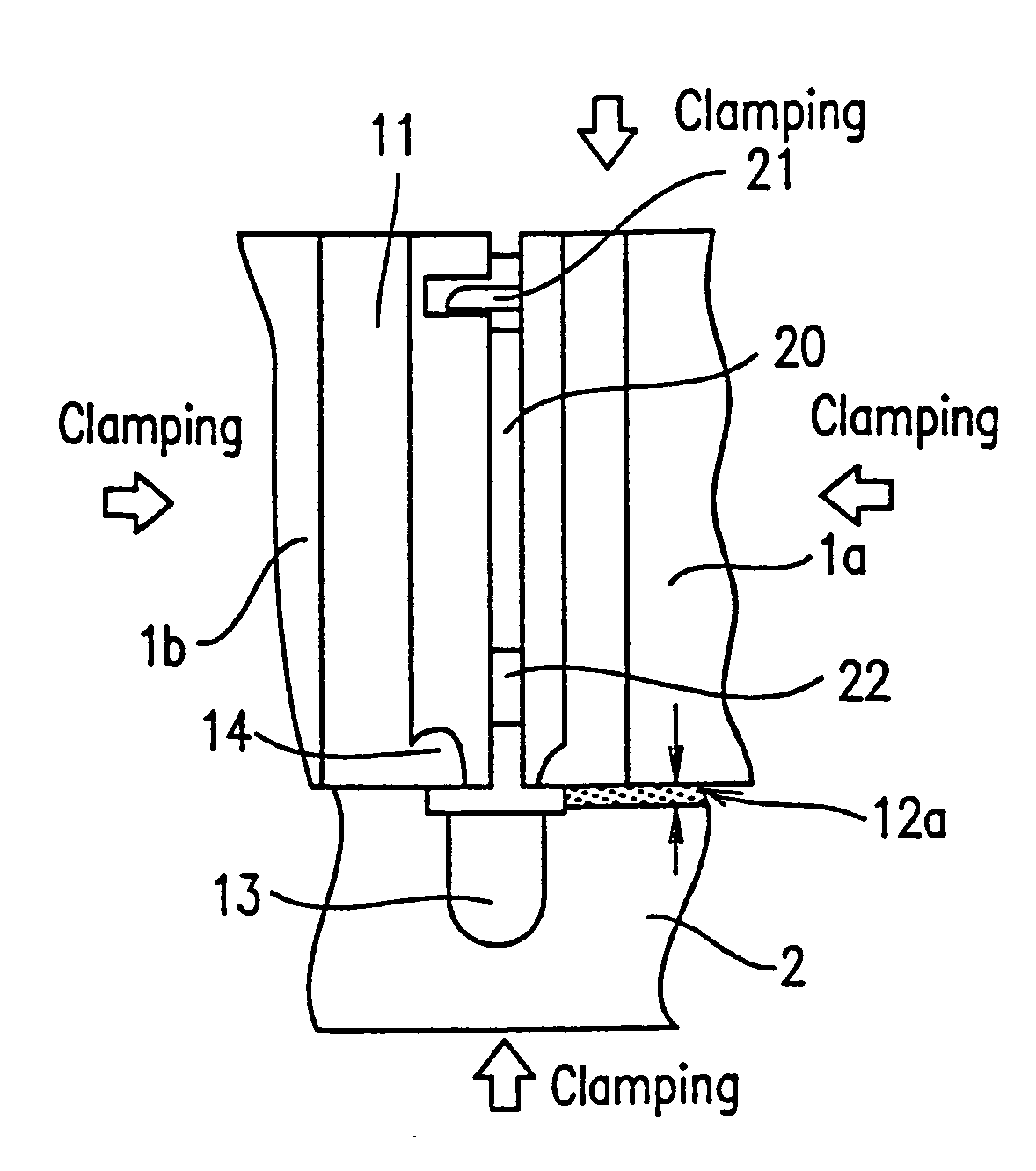
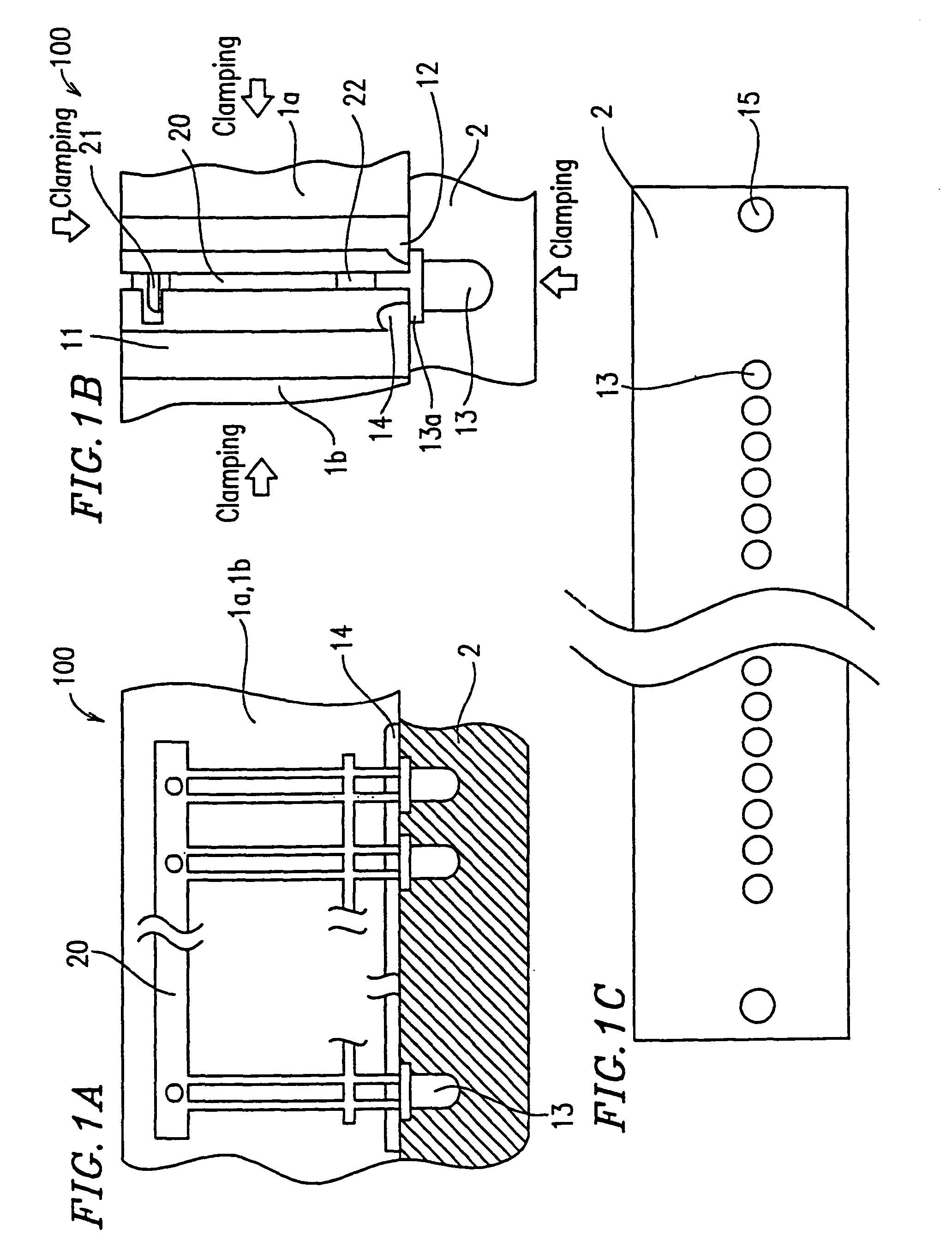
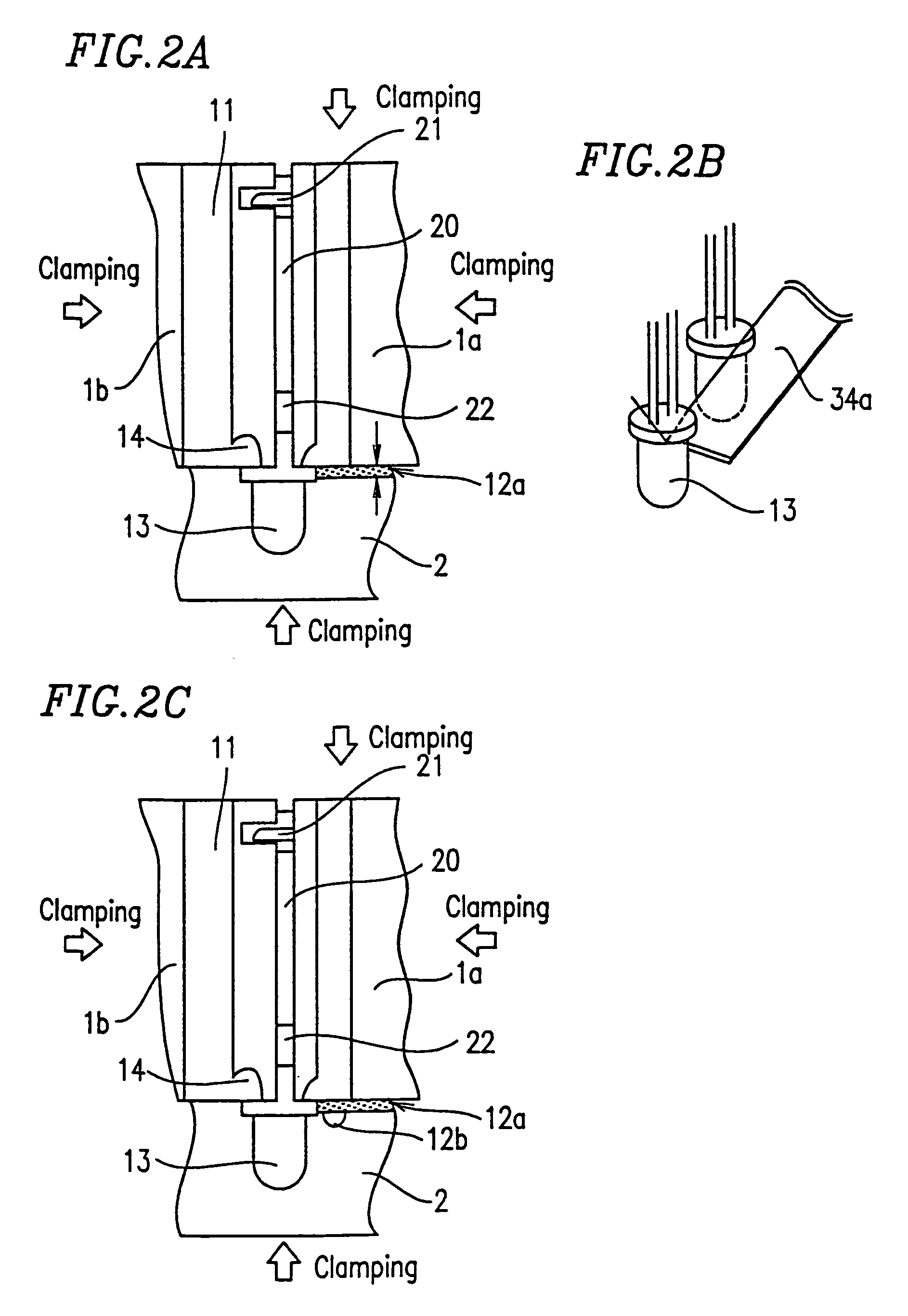
[0086]First, as shown in FIG. 6A, a lead frame 20 for an LED lamp, to which a semiconductor device has been mounted and wire-bonded, is positioned relative to a lead frame positioning pin 21 provided in an upper right die 1a. Then, an upper left die 1b is attached, and the upper right die 1a and the upper left die 1b are clamped together along the lateral direction. Then, the tip end of the lead frame 20 is inserted into a cavity 13 provided in a lower die 2, and the upper and lower dies 1a, 1b and 2 are clamped together along the vertical direction. An air vent 12 having a similar shape to that of the spool 11 is provided on the opposite side from the spool 11 with respect to the cavity 13. In Example 1 as well as Example 2 (described below), the spool 11 may have a diameter, e.g., Φ=about 5 mm, and the a...

example 2

[0094]In Example 2 of the present invention, a case will be described in which, in order to ensure stable resin injection from a single nozzle into multiple cavities, the temperature of the molding die is first lowered below the curing temperature of the resin used, and thereafter increased to or above the curing temperature of the resin.

[0095]First, as shown in FIG. 6A, a lead frame 20 for an LED lamp, to which a semiconductor device has been mounted and wire-bonded, is positioned relative to a lead frame positioning pin 21 provided in an upper right die 1a. Then, an upper left die 1b is attached, and the upper right die 1a and the upper left die 1b are clamped together along the lateral direction. Then, the tip end of the lead frame 20 is inserted into a cavity 13 provided in a lower die 2, and the upper and lower dies 1 and 2 are clamped together along the vertical direction.

[0096]Next, as shown in FIG. 6B, a cylindrical resin injection nozzle 30 is set to the spool 11. A space m...


PUM


Abstract

A resin molding die includes: a cavity; a resin inlet through which a liquid resin to be cured is injected into the cavity; and an air vent through which air is released to an exterior space of the resin molding die during injection of the resin, the air vent being provided on an opposite side from the resin inlet with respect to the cavity.

Description

[0001]This application is a divisional of application Ser. No. 09 / 799,360 filed Mar. 6, 2001 and now U.S. Pat. No. 6,652,795, the entire content of which is hereby incorporated by reference in this application.BACKGROUND OF THE INVENTION[0002]1. Field of the Invention[0003]The present invention relates to a resin molding die for use in the molding-based resin encapsulation of a semiconductor device, and a production method for semiconductor devices employing such a resin molding die. In particular, the present invention relates to a production method for semiconductor devices employing a high-fluidity liquid thermosetting resin as an encapsulation resin, and a resin molding die for use with such a production method.[0004]2. Description of the Related Art[0005]Conventionally, resin encapsulation of semiconductor devices is achieved by: (1) casting molding, (2) transfer molding, or (3) injection molding.[0006](1) Casting molding. This technique involves: pouring a liquid thermosetting...

Claims


Application Information

Patent Timeline
IPC IPC(8): B29C45/14H01L21/56B29C33/10B29C45/34B29C39/10B29C45/77B29C45/78B29K101/10B29L31/34
CPCB29C45/34H01L21/565Y10S425/812H01L2924/0002H01L2924/00
Inventor KONISHI, MASAHIROORITA, HIROKITAKADA, TOSHIYUKI
Owner SHARP KK
Features
  • R&D
  • Intellectual Property
  • Life Sciences
  • Materials
  • Tech Scout
  • Unparalleled Data Quality
  • Higher Quality Content
  • 60% Fewer Hallucinations
Learn More