Supercharge Your Innovation With Domain-Expert AI Agents!

Multi-level memory cell array with lateral floating spacers

a memory array and array technology, applied in semiconductor devices, digital storage, instruments, etc., can solve the problem of losing a part of the advantage of such a solution, and achieve the effect of increasing the vertical dimension

Inactive Publication Date: 2007-02-20
ATMEL CORP
View PDF5 Cites 1 Cited by
  • Summary
  • Abstract
  • Description
  • Claims
  • Application Information

AI Technical Summary

Benefits of technology

The patent describes a type of memory cell that uses two polysilicon floating spacers to store data bits. These spacers are separated from a central conductive gate by tunnel oxide and act as the main conductive charge storage. The structure is similar to a conventional EEPROM cell, but without increasing vertical dimensions. The charge is stored and isolated within the floating spacers using tunneling action. The control gate acts as a word line, while the subsurface source and drain regions are the digit lines connected to auxiliary transistors for independent control of each side of the memory cell. The technical effect of this invention is a more efficient and compact memory cell design with improved data storage and access.

Problems solved by technology

While use of multi-level memory chips would provide a solution, such chips are often larger than conventional transistors and so part of the advantage of such a solution is lost.

Method used


Image

  • Multi-level memory cell array with lateral floating spacers
  • Multi-level memory cell array with lateral floating spacers
  • Multi-level memory cell array with lateral floating spacers

Examples


Embodiment Construction

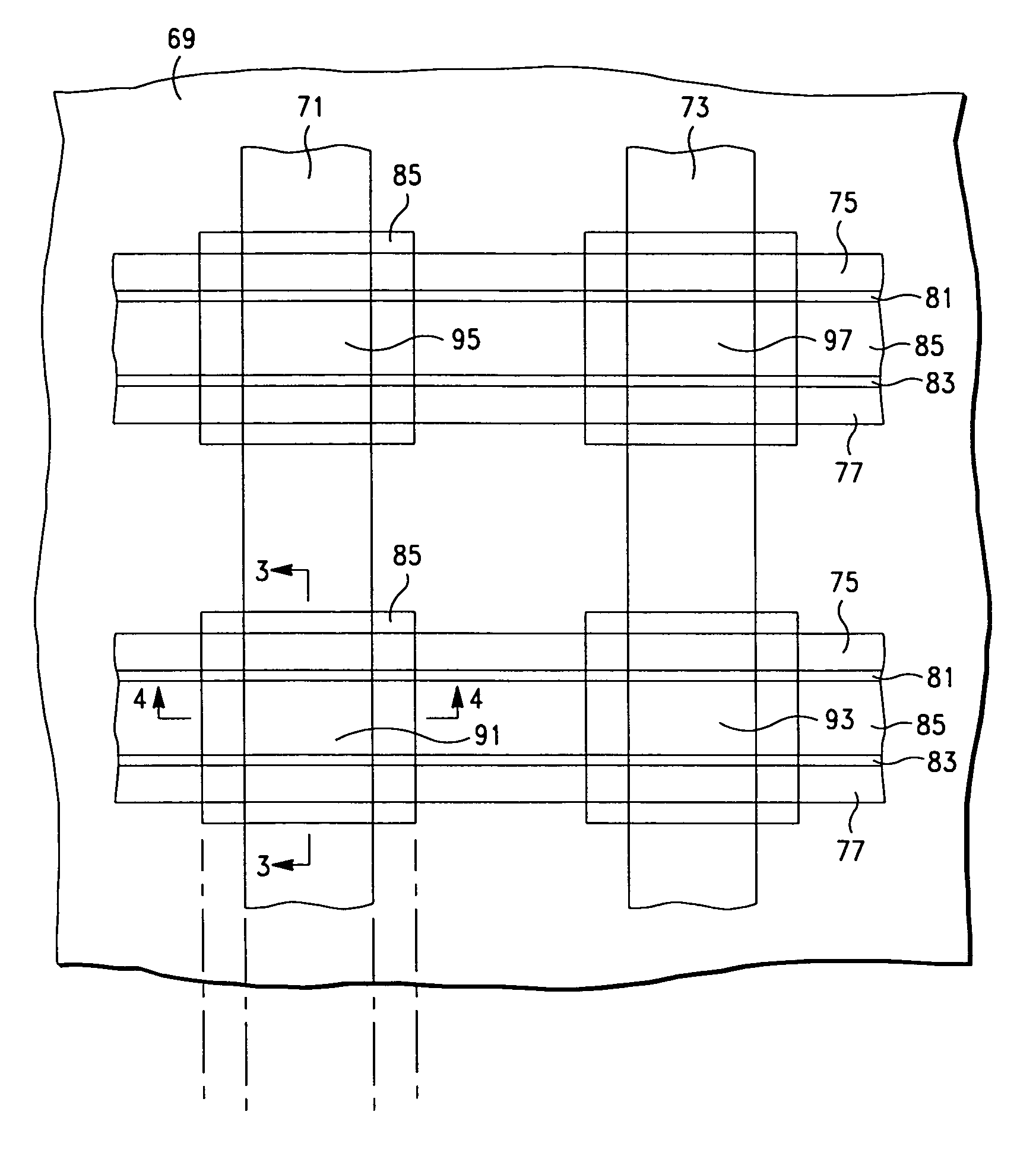
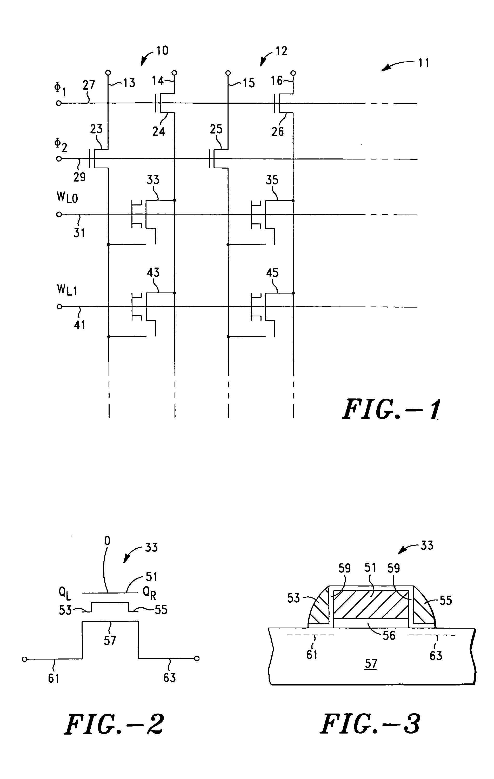
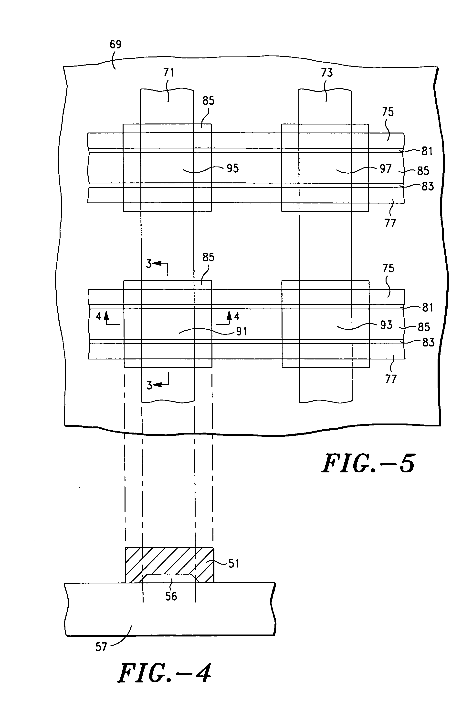
[0014]With reference to FIG. 1, a non-volatile memory array 11 is shown having memory array columns 10 and 12 with respective columnar lines 13 and 14 for array column 10 which, together, form a single bitline. Similarly, columnar lines 15 and 16 define a second bitline for array column 12. Between columnar lines 13 and 14 a first non-volatile memory transistor 33 and a second non-volatile memory transistor 43 are situated. In the second bitline, between columnar lines 15 and 16, third and fourth non-volatile memory transistors 35 and 45 are situated. Also associated with the first bitline are ancillary low voltage transistors 23 on timing line 29 and ancillary transistor 24 on timing line 27. Similarly, associated with the second bitline, ancillary low voltage transistor 25 is associated with timing line 29 and ancillary low voltage transistor 26 is associated with timing line 27. The function of the ancillary transistors will be explained below.

[0015]With reference to FIG. 2, the ...


PUM


Abstract

An array of multi-level non-volatile memory transistors features a transistor construction with a conductive polysilicon control gate having opposed sidewalls insulatively spaced just above the substrate. Conductive polysilicon spacers are separated from the opposed sidewalls by thin tunnel oxide. Source and drain implants are beneath or slightly outboard of the spacers. Insulative material is placed over the structure with a hole cut above the control gate for contact by a gate electrode connected to, or part of, a conductive word line. The array has auxiliary low voltage transistors which may be made at the same time as the formation of the memory transistors. The auxiliary transistors apply opposite phase clock pulses to source and drain electrodes of transistors in the array so that first one side of each memory transistor may be written to, or read, then the other side.

Description

CROSS-REFERENCE TO RELATED APPLICATION[0001]This is a divisional of application Ser. No. 10 / 327,336 filed Dec. 20, 2002 now U.S. Pat. No. 6,831,325.TECHNICAL FIELD[0002]The invention relates to semiconductor integrated memory cells and, in particular, to multibit charge storage transistors in a memory array.BACKGROUND ART[0003]In the past, nonvolatile memory transistors stored only one binary bit. In EEPROM (electrically eraseable programmable read only memory) transistors such charge storage occurs on a floating gate and so, such transistors are referred to as floating gate memory cell transistors. In order to store two binary bits in an EEPROM transistor, some modification of the transistor design is needed. Multibit charge storage transistors are known, including nonvolatile multibit transistors.[0004]In U.S. Pat. No. 6,323,088, Gonzalez et al. teach the use of two floating gates, placed side-by-side, beneath a control gate to form a multi-level memory cell. The control gate is c...

Claims


Application Information

Patent Timeline
Patent Type & Authority Patents(United States)
IPC IPC(8): H01L29/788H01L29/76H10B12/00H01L21/28H01L21/8247H01L29/423H10B69/00
CPCH01L21/28273H01L27/105H01L27/115H01L29/7887H01L27/11526H01L27/11546H01L29/42332H01L27/11521H01L29/40114H10B69/00H10B41/30H10B41/40H10B41/49H01L29/66825
Inventor LOJEK, BOHUMIL
Owner ATMEL CORP
Features
  • R&D
  • Intellectual Property
  • Life Sciences
  • Materials
  • Tech Scout
  • Unparalleled Data Quality
  • Higher Quality Content
  • 60% Fewer Hallucinations
Learn More