High performance low power multiple-level-switching output drivers

a high-performance, output driver technology, applied in logic circuits, pulse techniques, oscillators, etc., can solve the problems of reducing the power consumption of sai drivers, limiting the support of cmos drivers for high-performance interfaces, and i/o bandwidth becoming the performance bottleneck of high-performance systems, etc., to achieve low power consumption, avoid switching noise problems, and high-performance operations.

Inactive Publication Date: 2007-02-20
UNIRAM TECH
View PDF4 Cites 20 Cited by
  • Summary
  • Abstract
  • Description
  • Claims
  • Application Information

AI Technical Summary

Benefits of technology

[0009]The primary objective of this invention is, therefore, to provide output drivers that consume little power at steady state while avoiding switching noise problems to support high performance operations. The other primary objective of this invention is to provide output drivers that can switch between multiple levels of high accuracy output voltages while consuming minimum power. Another objective is to support small amplitude interface protocols without using termination resistors. These and other objectives are achieved by using output drivers comprising n-channel pull up transistors and p-channel pull down transistors bias with proper gate voltages. The resulting circuits are capable of supporting high performance synchronized signals or high accuracy multiple level signals while consuming much less power than prior art options.

Problems solved by technology

Otherwise, input / output (I / O) bandwidth would become the performance bottleneck in high performance systems.
However, switching noise related problems limited CMOS drivers in supporting high performance interfaces.
However, SAI drivers consume power even when they are not switching data, and they still suffer most of the noise problems suffered by conventional CMOS drivers.
Wireless devices such as cellular phones have progressed in explosive pace.
Most of prior art digital-to-analog converters use operation amplifiers with negative feedback to provide high accuracy output signals, but operation amplifiers typically consume a lot of power and have poor switching speed.
The pre-charge operation will consume power no matter the data is changed or not.
Since Tsuchi only use pull down driver, the method is sensitive to noises that cause the output signal to drop below targeted voltages.

Method used


Image

  • High performance low power multiple-level-switching output drivers
  • High performance low power multiple-level-switching output drivers
  • High performance low power multiple-level-switching output drivers

Examples


Embodiment Construction

[0019]The operation principles of prior art output drivers are first discussed to facilitate clear understanding of the present invention.

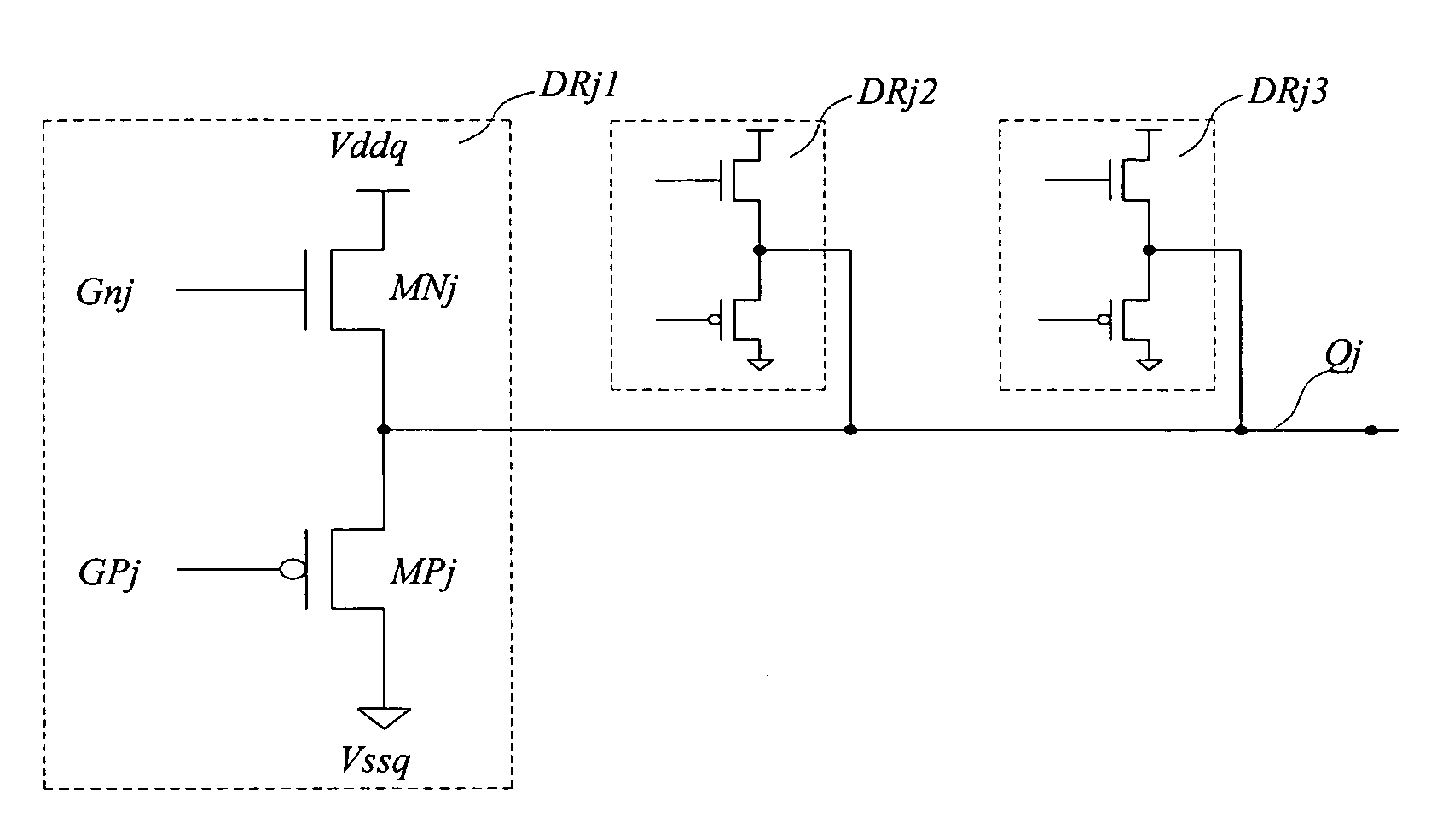
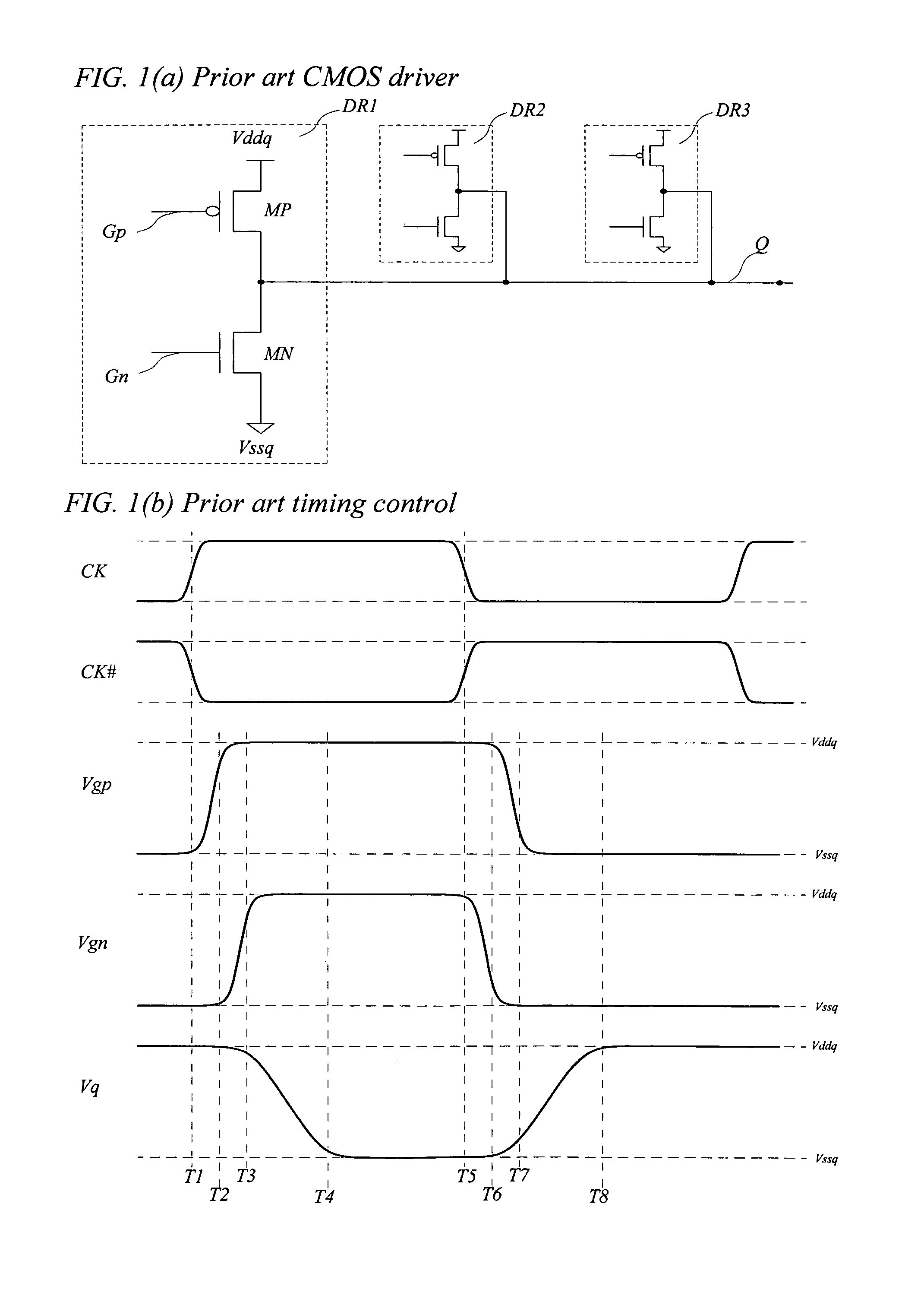
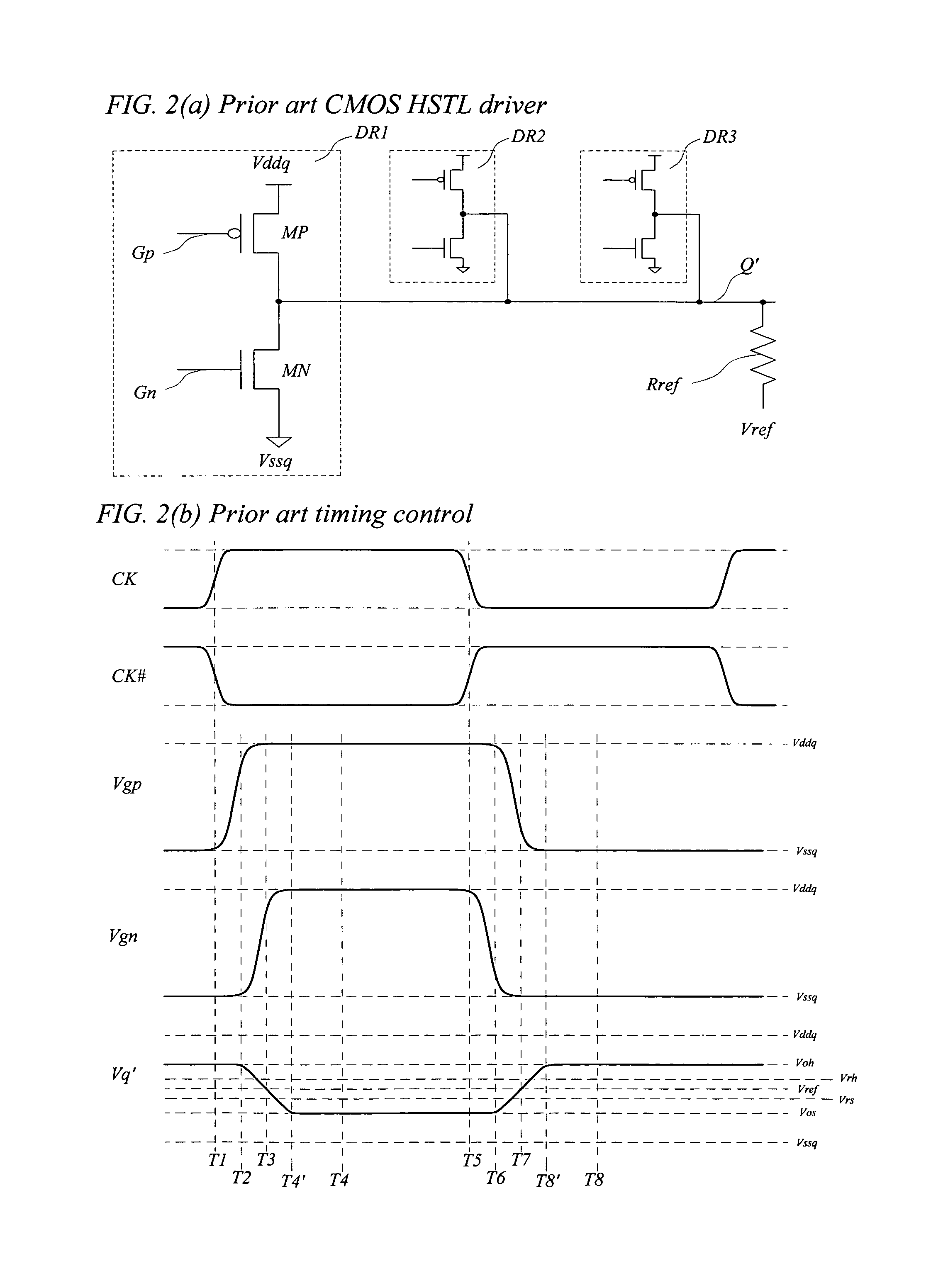
[0020]FIG. 1(a) is a schematic diagram showing the basic elements of a prior art CMOS output driver (DR1). An output driver is defined as the last-stage circuit used to drive output signals from an IC to external components. A high performance output driver defined in this patent disclosure is the last-stage circuit used to drive high performance switching signals from an IC to external components while it is designed to support output signal switching rate higher than thousands, millions, or even billions of cycles per second. This prior art output driver (DR1) comprises a p-channel pull up transistor (MP) and an n-channel pull down transistor (MN). A pull up transistor is defined as a transistor configured to provide channel current in a direction to pull the output signal only to higher voltage. A pull down transistor is defined as a transistor...


PUM


Abstract

Long existing performance, noise, and power consumption problems of prior art output drivers are solved by using n-channel transistors as pull up transistors and p-channel transistors as pull down transistors for high performance output drivers. Output drivers of the present invention can be fully compatible with HSTL or SSTL interfaces without using termination resistors. High resolution switching applications are also made possible without consuming much power. Output drivers of the present invention provide excellent solutions to support high performance interface while consuming much lower power.

Description

BACKGROUND OF THE INVENTION[0001]1. Field of the Invention[0002]The present invention relates to output drivers for integrated circuits (IC), and more particularly to low power, high performance output drivers designed to drive multiple-level switching partial-voltage signals.[0003]2. Description of the Prior Art[0004]Today, IC technologies have progressed into nanometer (nm) ranges. Current art 65 nm logic technologies provide transistors with switching time measured by 10−12 seconds (ps). It has become a routine practice to design logic circuits capable of executing billions or even trillions of operations per second. Such powerful core circuits require the supports of powerful interface circuits. Otherwise, input / output (I / O) bandwidth would become the performance bottleneck in high performance systems. It is therefore highly desirable to provide methods to improve the performance of I / O circuits for integrated circuits.[0005]An output driver, by definition, is the last-stage cir...

Claims


Application Information

Patent Timeline
Patent Type & Authority Patents(United States)
IPC IPC(8): H03B1/00
CPCH03K19/09485H03K19/018521
Inventor SHAU, JENG-JYE
Owner UNIRAM TECH
Why Eureka
Try Eureka