Supercharge Your Innovation With Domain-Expert AI Agents!

Bilayer aluminum last metal for interconnects and wirebond pads

a wirebond pad and aluminum technology, applied in the direction of semiconductor devices, semiconductor/solid-state device details, electrical apparatus, etc., can solve the problems of unsatisfactory, unsatisfactory, and difficult reduction of wirebond ball size from 70 m to 50 m, and increase the thickness of the last wire bonding level to approximately 1 m

Inactive Publication Date: 2007-02-27
INT BUSINESS MASCH CORP
View PDF9 Cites 4 Cited by
  • Summary
  • Abstract
  • Description
  • Claims
  • Application Information

AI Technical Summary

Benefits of technology

The present invention provides an improved method and structure for connecting wirebonds with ball size of approximately 50 μm and smaller to the last metal interconnect on a microelectronic device. This allows for a more efficient and effective connection between the wirebond and the device. The structure includes a substrate with a microelectronic circuit and a wiring layer over the substrate, which includes a bilayer wiring structure comprising upper and lower electrically conductive layers separated by a protective electrically conductive layer. The wirebond is connected to the upper layer of the bilayer structure. The invention also includes a method for making the electronic device structure. The wiring layer has a thickness no greater than about 500 nm, and the upper and lower layers of the bilayer structure have substantially the same thickness as the wiring level. The protective layer has a thickness substantially less than the upper and lower layers of the bilayer structure, preferably about 10 to 100 nm, and is a refractory selected from the group consisting of TiN, TaN, TiSiN, WN, W, Ta, TiAl or combinations therof.

Problems solved by technology

The decrease in wirebond ball size from 70 μm to 50 μm has been difficult because of the aforementioned decrease in metal layer thickness.
One solution to this problem, increasing the thickness of the last wiring level to approximately 1 μm, is not desirable because with the wire width in the 200–400 nm size, the aspect ratio and capacitance of this last wiring level would be unacceptably high.
However this adds significant cost.

Method used


Image

  • Bilayer aluminum last metal for interconnects and wirebond pads
  • Bilayer aluminum last metal for interconnects and wirebond pads
  • Bilayer aluminum last metal for interconnects and wirebond pads

Examples


Embodiment Construction

)

[0027]In describing the preferred embodiment of the present invention, reference will be made herein to FIGS. 1–12 of the drawings in which like numerals refer to like features of the invention.

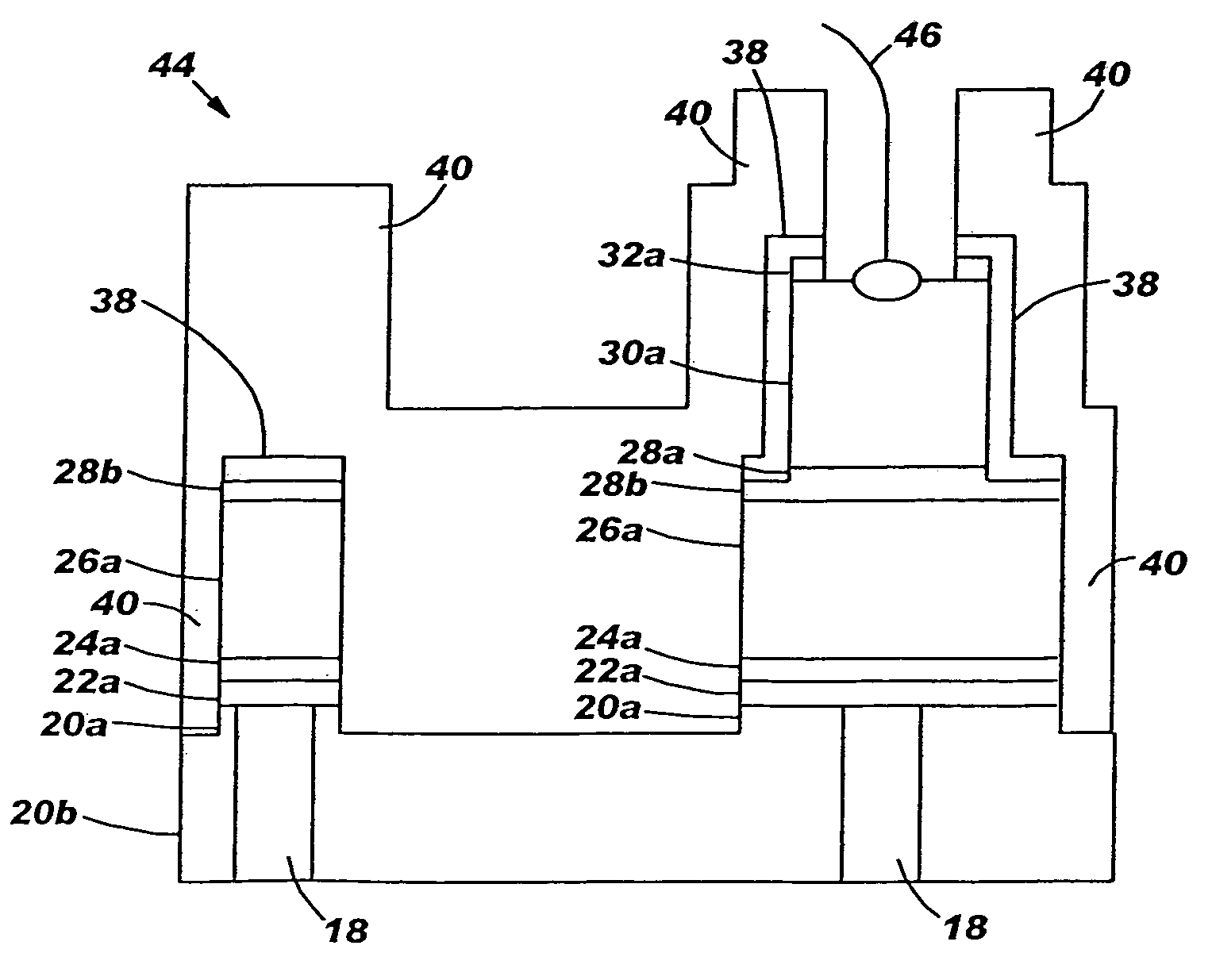
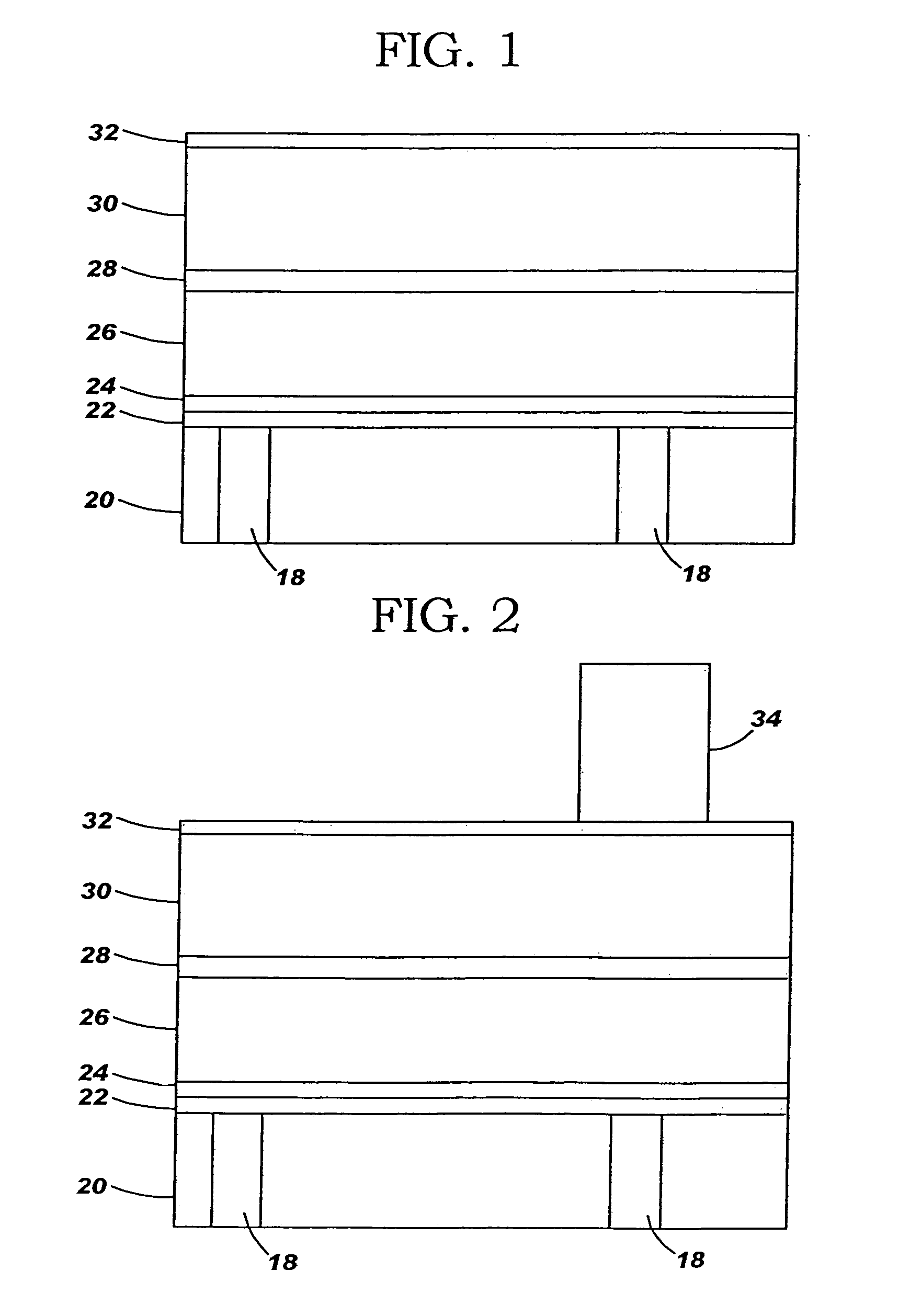
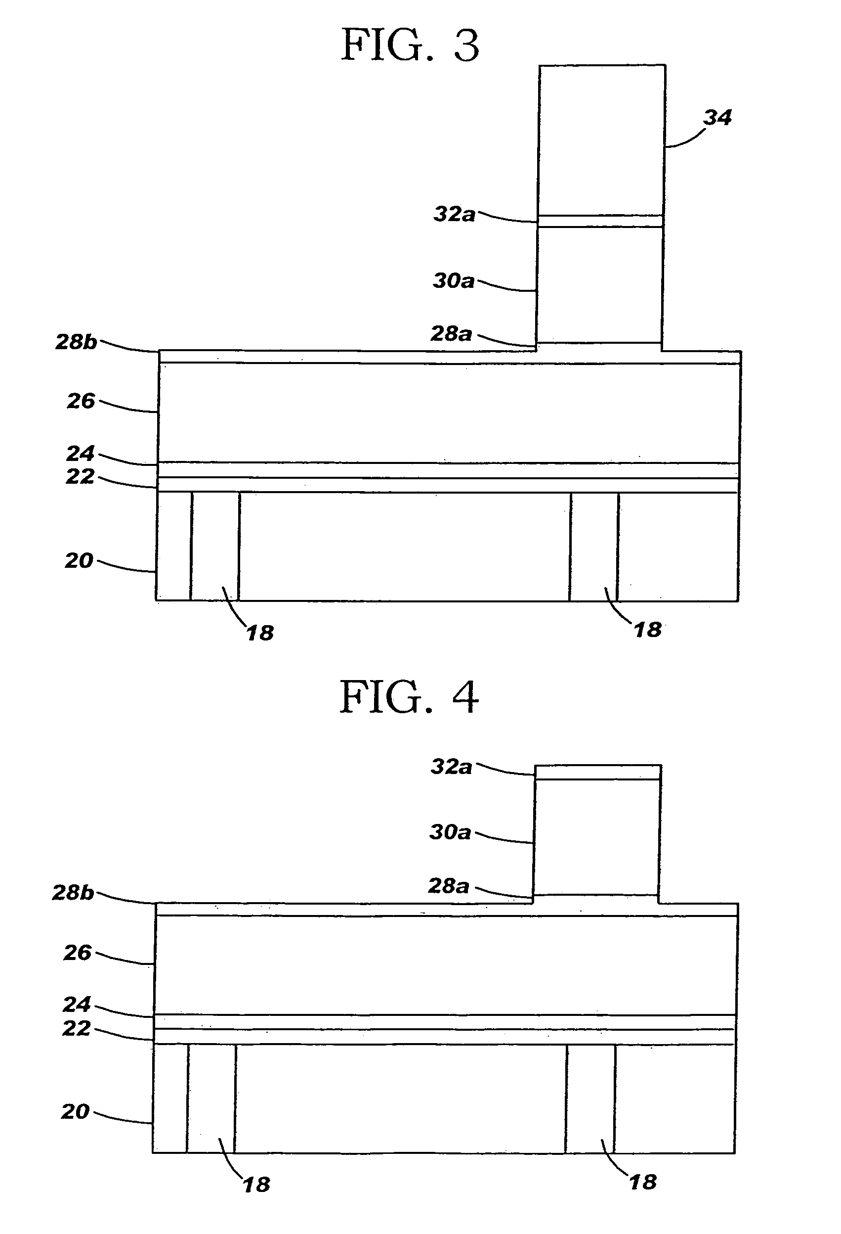
[0028]Instead of i) adding additional wiring levels only for the wirebond and / or ii) creating an unacceptable high thickness of the last aluminum copper wiring level, the present invention provides a dual thickness last wiring level with on-pitch wires, e.g. wires approximately 500 nm high, and wirebond pads of approximately greater than twice the height, e.g., approximately 1 μm or thicker. The present invention may be used to fabricate dual height wiring of any desired thickness for any purpose.

[0029]As shown in FIG. 1, the double layer metal stack comprises an underlying substrate layer 20, a titanium layer 22, here shown as being approximately 25 nm thick, and superimposed thereover a titanium nitride (TiN) layer 24, also shown as approximately 25 nm thick. The materials used for layers ...


PUM


Abstract

A method for connecting a microelectronic device to a wirebond comprises providing a substrate having a microelectronic circuit therein and forming a wiring layer over the substrate. The wiring layer includes a bilayer wiring structure comprising upper and lower electrically conductive layers separated by a protective electrically conductive layer. The lower layer of the bilayer structure is at the level of the wiring layer and the upper layer of the bilayer structure extends above the level of the wiring layer. The bilayer wiring structure is formed by depositing the upper and lower electrically conductive layers separated by a protective electrically conductive layer over the substrate, etching the upper electrically conductive layer and a portion of the protective electrically conductive layer, and thereafter separately etching the lower electrically conductive layer to form the wiring layer over the substrate. The method also includes connecting a wirebond to the upper layer of the bilayer structure.

Description

BACKGROUND OF THE INVENTION [0001]1. Field of the Invention[0002]The present invention relates to the packaging of integrated circuits and, in particular, to a structure and method for making wirebond connections to microelectronic devices.[0003]2. Description of Related Art[0004]Wirebond connections are made to wiring levels of microelectronic devices in order to electrically connect the circuits of the microelectronic device to a larger connector formed in the package supporting the microelectronic device. With decreasing size of circuitry on microelectronic devices, wirebond balls have likewise diminished in size. With microelectronic device wiring level thickness now being at the level of approximately 500 nm and wire widths in the range of about 300–400 nm, wirebond ball sizes have also decreased. The decrease in wirebond ball size from 70 μm to 50 μm has been difficult because of the aforementioned decrease in metal layer thickness. These 50 μm wirebonds have in some cases bee...

Claims


Application Information

Patent Timeline
Patent Type & Authority Patents(United States)
IPC IPC(8): H01L23/48H01L23/52H01L29/40
CPCH01L21/76885H01L24/05H01L24/48H01L2924/01033H01L2924/00014H01L2924/30105H01L2224/04042H01L2224/05624H01L2224/48463H01L2224/85424H01L2924/01005H01L2924/01013H01L2924/01014H01L2924/01022H01L2924/01029H01L2924/0105H01L2924/01073H01L2924/01074H01L2924/04941H01L2924/04953H01L2924/05042H01L2924/14H01L2924/19042H01L2224/45099H01L2224/02166
Inventor LUCE, STEPHEN E.MCDEVITT, THOMAS L.STAMPER, ANTHONY K.
Owner INT BUSINESS MASCH CORP
Features
  • R&D
  • Intellectual Property
  • Life Sciences
  • Materials
  • Tech Scout
  • Unparalleled Data Quality
  • Higher Quality Content
  • 60% Fewer Hallucinations
Learn More