Organic light-emitting diode for display and method for fabricating the same

a light-emitting diode and organic technology, applied in the direction of discharge tube luminescnet screen, other domestic articles, natural mineral layered products, etc., can solve the problems of undesirable heat development, cathode may be damaged by the pressure, and the cathode structure disadvantageously increases the electrical resistance, so as to reduce the contact resistance and less power

Inactive Publication Date: 2007-03-20
SAMSUNG DISPLAY CO LTD
View PDF6 Cites 5 Cited by
  • Summary
  • Abstract
  • Description
  • Claims
  • Application Information

AI Technical Summary

Benefits of technology

[0015]The present invention provides an organic light-emitting diode (OLED) for a display that has a reduced contact resistance between a cathode and a cathode contact layer and requires a less amount of power at a given capacity, and a method of fabricating the OLED.

Problems solved by technology

When the FPC is directly bound to the cathode by hot sealing, the cathode may be damaged by the pressure and the temperature applied to seal and bind the FPC to the cathode.
However, this cathode structure disadvantageously increases electrical resistance gradually as a current flows along the cathode lines.
A greater electrical resistance caused by the cathode requires a larger amount of power to operate an OLED or a display employing such a cathode, so that undesirable heat development occurs in the OLED or the display.

Method used


Image

  • Organic light-emitting diode for display and method for fabricating the same
  • Organic light-emitting diode for display and method for fabricating the same

Examples


Embodiment Construction

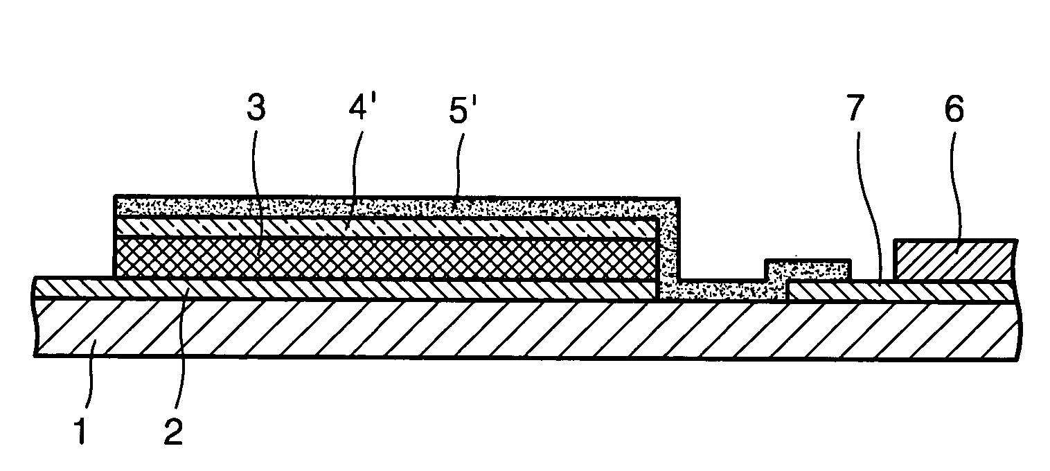
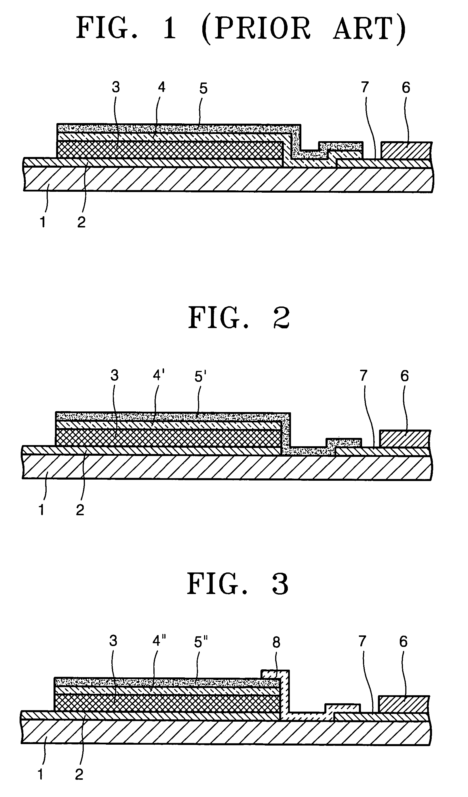
[0029]An organic light-emitting diode (OLED) and a method for fabricating the same according to the present invention will be described with the following exemplary embodiments and with reference to the accompanying drawings.

[0030]A multi-layered cathode has a greater contact resistance with respect to a cathode contact layer formed of indium tin oxide (ITO), than a single layered aluminum cathode, for example. To compare the contact resistance of different arrangements, it is assumed that a single layered cathode formed of a 500-nm-thick aluminum layer has about 100% contact resistance with respect to the ITO cathode contact layer. Using that arrangement and contact resistance as a marker, a multi-layered cathode including a 1-nm-thick lithium chloride layer, a 10-nm-thick calcium layer, and a 500-nm-thick aluminum layer has a relative contact resistance of about 111%, a cathode including a 1-nm-thick lithium chloride layer and a 500-nm-thick aluminum layer has a relative contact r...


PUM

PropertyMeasurementUnit
thicknessaaaaaaaaaa
thicknessaaaaaaaaaa
electrical conductingaaaaaaaaaa

Abstract

An organic light-emitting diode for a display and a method for fabricating the organic light-emitting diode which has lower contact resistance between the cathode and the cathode contact layer and which may be operated with a reduced amount of power. The organic light-emitting diode has an anode layer, an emissive layer, a cathode which has an electron injecting layer and an electrical conducting layer, and a cathode contact layer which electrically connects the cathode and an electrical driving system of the display. The electrical conducting layer of the cathode is electrically connected with the cathode contact layer, however, the electron injecting layer is not in direct contact with the cathode contact layer. Both the electron injecting layer and the electrical conducting layer of the cathode may be formed such that they are aligned with the emissive layer. In this case, a connecting layer is formed to connect the electrically conducting layer and the cathode contact layer.

Description

[0001]This application claims priority from German Patent Application 02 090 368.8, filed on Nov. 6, 2002 in the German Patent Office and Korean Patent Application 2003-11591, filed on Feb. 25, 2003 in the Korean Intellectual Property Office, the disclosures of which are incorporated herein in their entirety by reference.BACKGROUND OF THE INVENTION[0002]1. Field of the Invention[0003]This invention relates to an organic light-emitting diode, for a display, with low cathode contact resistance, and a method for fabricating the same.[0004]2. Description of the Related Art[0005]Displays using an organic light-emitting diode (OLED) provide great brightness and a wide viewing angle. OLEDs are self-luminous so they do not require back light and can be effectively used even under relatively dark ambient conditions.[0006]OLEDs include an organic semiconductor layer which acts as an emissive layer between two electrodes. At least one of these electrodes is formed of transparent material.[0007...

Claims


Application Information

Patent Timeline
Patent Type & Authority Patents(United States)
IPC IPC(8): H05B33/12H01L51/50H05B33/06H01L33/00H05B33/10H05B33/14H05B33/22
CPCH01L27/3288H01L51/5221Y10S428/917H10K59/179H10K50/826H05B33/06
Inventor ALBRECHT, UHLIGJOERG, FISCHERANDREAS, ZABEL
Owner SAMSUNG DISPLAY CO LTD
Why Eureka
Try Eureka