Bandgap reference voltage circuit

a reference voltage and circuit technology, applied in pulse generators, instruments, pulse techniques, etc., can solve the problems of source-drain voltage vsd of the third metal oxide semiconductor field effect transistor mb>3/b>, and the voltage vreg would decreas

Active Publication Date: 2007-03-20
ANALOG INTEGRATIONS CORP
View PDF5 Cites 27 Cited by
  • Summary
  • Abstract
  • Description
  • Claims
  • Application Information

AI Technical Summary

Benefits of technology

[0007]The main aspect of the present invention is to provide a bandgap reference voltage circuit, in which the source-drain voltage of the metal oxide semiconductor field effect transistor which electrically connected to an output terminal of the bandgap reference voltage circuit falling into a triode region is prevented, so that the temperature compensation effect is able to be executed and thus the provide normally bandgap reference voltage is stable.

Problems solved by technology

However, the disadvantage of the bandgap reference voltage circuit 10 shown in FIG. 1(a) is that the voltage VREG would decrease with the rising temperature while the bandgap reference voltage VBG still remains as a constant, which makes the source-drain voltage VSD of the third metal oxide semiconductor field effect transistor M3 decrease substantially.

Method used


Image

  • Bandgap reference voltage circuit
  • Bandgap reference voltage circuit
  • Bandgap reference voltage circuit

Examples


Embodiment Construction

[0032]The present invention will now be described more specifically with reference to the following embodiments. It is to be noted that the following descriptions of preferred embodiments of this invention are presented herein for purpose of illustration and description only, it is not intended to be exhaustive or to be limited to the precise form disclosed.

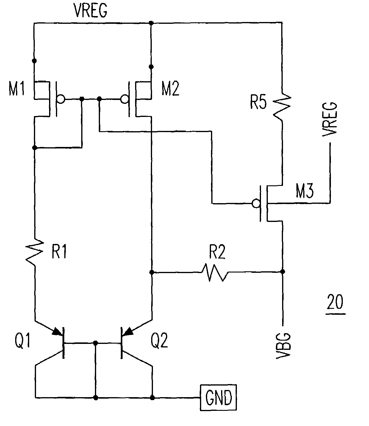
[0033]Please refer to FIG. 2, which schematically shows a bandgap reference voltage circuit according to a first preferred embodiment of the present invention. As shown in FIG. 2, the bandgap reference voltage circuit 20 includes three p-typed metal oxide semiconductor field effect transistors M1, M2 and M3, three resistors R1, R2 and R5, and two pnp-typed bipolar junction transistor Q1 and Q2.

[0034]The first metal oxide semiconductor field effect transistor M1 has a first source electrically connected to a relatively high voltage VREG, and a first gate electrically connected to a first drain thereof. The second metal oxide semic...


PUM


Abstract

A bandgap reference voltage circuit is provided, in which an additional resistor as well as a transistor is utilized to prevent the source-drain voltage of a metal oxide semiconductor field effect transistor electrically connected to an output terminal of the bandgap reference voltage circuit from falling into the triode region. Through the provided bandgap reference voltage circuit, the temperature compensation effect is able to be normally executed, so as to supply a stable bandgap reference voltage.

Description

FIELD OF THE INVENTION[0001]The present invention relates to a bandgap reference voltage circuit, and more particular to a bandgap reference voltage circuit with a perfect temperature compensation effect at a rising temperature.BACKGROUND OF THE INVENTION[0002]In the technical report entitled “A Low Supply Voltage High PSRR Voltage Reference in CMOS Process” by Khong-Meng Tham and Krishnaswamy Nagaraj, a conventional bandgap reference voltage circuit 10 is disclosed, as shown in FIG. 1(a). The bandgap reference voltage circuit 10 includes a first, a second and a third p-typed metal oxide semiconductor field effect transistors (MOSFETs) M1, M2 and M3, a first and a second pnp-typed bipolar junction transistors (BJTs) Q1 and Q2, and a first and a second resistors R1 and R2. In this case, the pn junction area ratio of the first pnp-typed bipolar junction transistor Q1 is equal to M multiplied by that of the second pnp-typed bipolar junction transistor Q2, in which M is an integer great...

Claims


Application Information

Patent Timeline
Patent Type & Authority Patents(United States)
IPC IPC(8): G05F3/24
CPCG05F3/30Y10S323/907
Inventor LEE, JIAN-LUNGWU, TSUNG-HSIU
Owner ANALOG INTEGRATIONS CORP
Why Eureka
Try Eureka