Semiconductor memory device and write/readout controlling method error correction code decoding device

a memory device and memory technology, applied in the direction of digital storage, instruments, transistors, etc., can solve the problems of increasing the bit line length, difficult high-speed operation, and the memory device of the semiconductor is not up to high-speed operation

Inactive Publication Date: 2003-06-26
RENESAS ELECTRONICS CORP
View PDF2 Cites 17 Cited by
  • Summary
  • Abstract
  • Description
  • Claims
  • Application Information

AI Technical Summary

Benefits of technology

0009] Accordingly it is an object of the present invention to provide a programmable semiconductor memory device, employing an electrically conductive layer as an impurity layer, in which the resistance value of the electrically conductive layer by the impurity layer may be diminished and in which the selecting transistors may be of the high voltage withstand type.

Problems solved by technology

However, such semiconductor memory device is not up to high-speed operations, due to bit-line resistance or stray capacitance, because the bit lines are formed by impurity doped electrically conductive areas provided on a silicon substrate.
The bit line length is increased due to increased storage capacity to render the high speed operation difficult.
If the transistor is of the high voltage withstand type to diminish the on-resistance and to suppress the lowering of the current at the time of writing, the junction withstand voltage characteristics are lowered in an impurity layer serving for device isolation across the selecting transistors, thus causing breakdown of the selecting transistor.

Method used


Image

  • Semiconductor memory device and write/readout controlling method error correction code decoding device
  • Semiconductor memory device and write/readout controlling method error correction code decoding device
  • Semiconductor memory device and write/readout controlling method error correction code decoding device

Examples


second embodiment

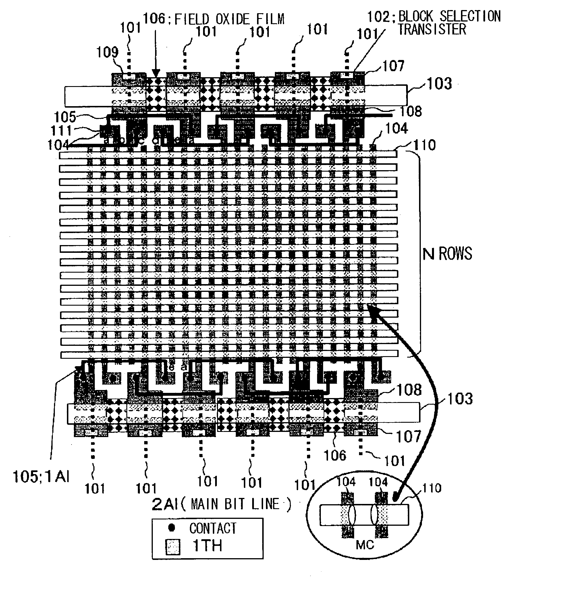
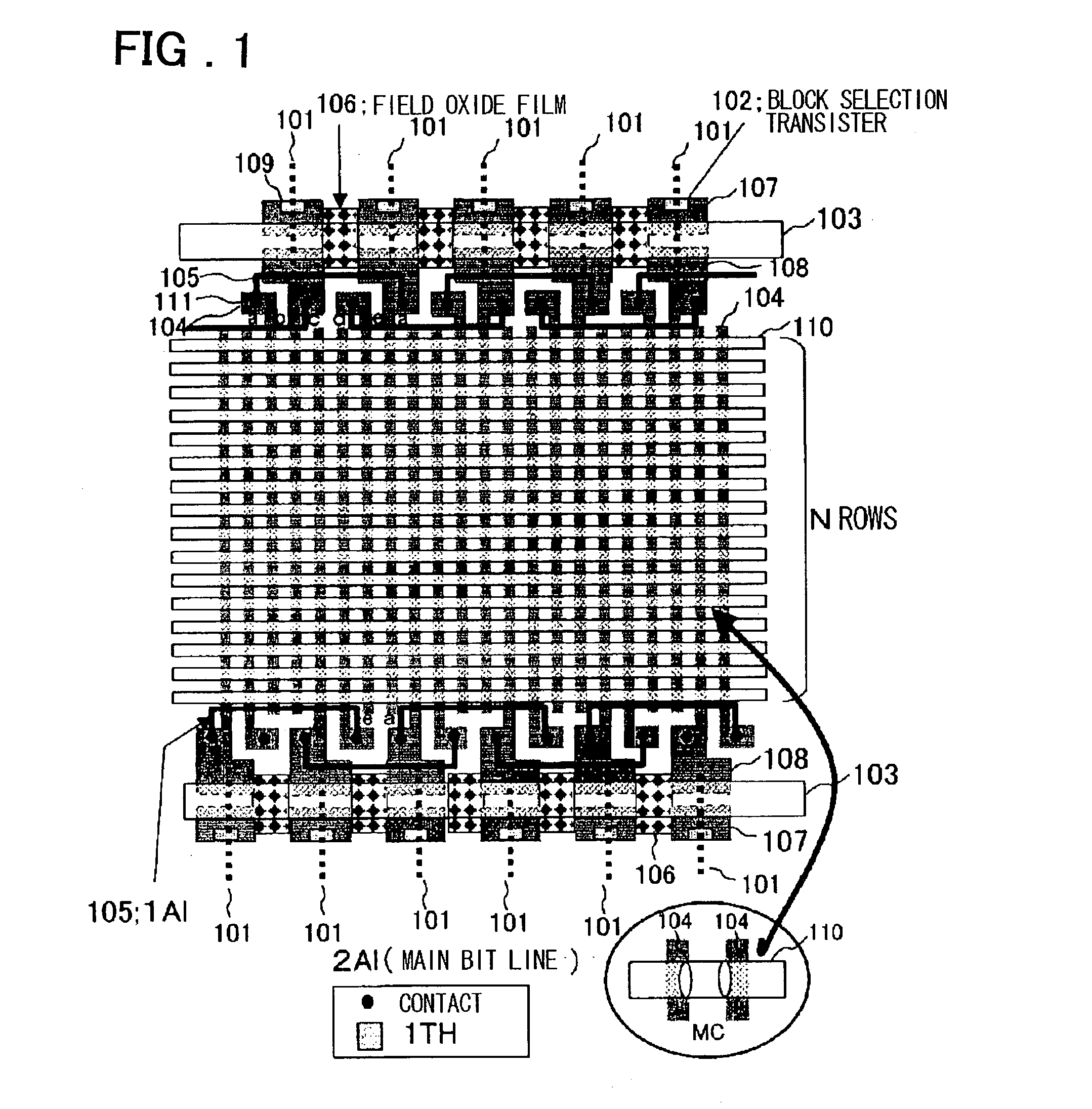
[0117] An alternative embodiment of the present invention is now explained. FIG. 10 is a diagram showing a layout structure according to the present invention. The embodiment shown in FIG. 10 corresponds to the structure shown in FIG. 1 in which the ends at the other end of the memory cell array of the paired electrically conductive regions 104, connected at an end of the memory cell array to the wiring 105 via contact 111, are also connected via contact 111 to the wiring 105 of the first aluminum wiring layer 1A1. By connecting the paired electrically conductive regions 104, forming the sub bit lines, at both of the longitudinal ends thereof, it is possible to reduce the resistance of the electrically conductive regions 104 connecting to the memory cells.

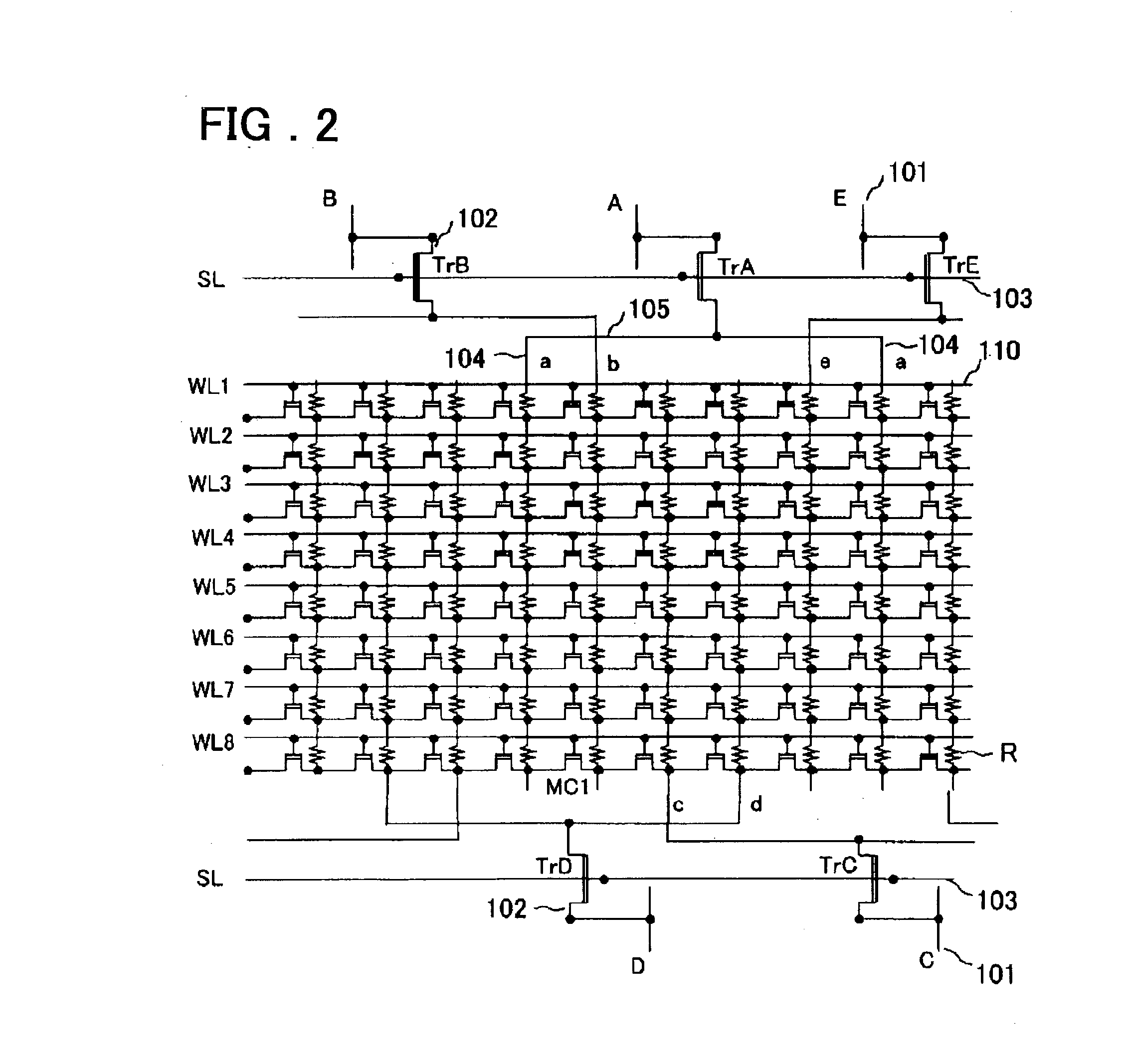
[0118] FIG. 11 is a diagram showing a circuit configuration of a memory cell array according to the second embodiment of the present invention, an illustrative layout of which is shown in FIG. 10. Referring to FIG. 11, the circuit ...

first embodiment

[0121] With the memory cell remotest from the selecting transistor, n=8, at which time the resistance value of the sub bit line is 4R or one half the resistance in the case of the

[0122] In the present embodiment, programming and readout occur as measures are taken to prevent writing in other cells during programming, to prevent the decreasing write current, to prevent the current leakage in the reverse direction during readout and to reduce the interference current.

[0123] FIG. 12 shows a structure according to a third embodiment of the present invention. In the present embodiment, the paired electrically conductive regions, connected to the wiring 105 of the first aluminum wiring layer 1A1 via contact 111 at one longitudinal end of the memory cell array have the opposite side longitudinal ends connected to the wiring 105 of the first aluminum wiring layer 1A1 through the contact 111, as in the second embodiment described above. In addition, the longitudinal ends of the respective el...

third embodiment

[0127] FIG. 13 shows an equivalent circuit of a memory cell array according to the present invention, an illustrative layout of which is shown in FIG. 12. In each of the paired electrically conductive regions, an end connected to the selection transistor 102 is connected via wiring 112 to its own longitudinally opposite end. The longitudinally opposite ends of the remaining electrically conductive regions are similarly connected to each other via a wiring 112 on the upper substrate layer.

[0128] The resistance value of the electrically conductive region in the memory cell of the selected nth row, when looking from the selecting transistor, is a parallel resistance of nR and (8-n)R, such that we have as a combined resistance n(8-n)R / 8.

[0129] With the remotest memory cell, when looking from the selecting transistor, n=8, in which case the resistance value of the sub bit line is 0. The row with the maximum resistance value is n=4, with the resistance value being 2R.

[0130] In the present...


PUM


Abstract

Disclosed are device and method for enabling a programmable semiconductor memory device to provide a block selection transistor of a high voltage withstand type, to prevent the voltage from being decreased at the time of programming and to prevent the readout current from being decreased and to provide a constant sum resistance of the electrically conductive regions without dependency upon the memory cell locations. In a pair of two electrically conductive regions, provided for extending parallel to and in separation from each other on a substrate surface, one longitudinal end of one of the electrically conductive regions is diagonally connected to the other longitudinal end of the other electrically conductive region by a wiring to form a set of sub bit lines. On both ends of the memory cell array, there are provided selection transistors for interconnecting the sub bit lines and main bit lines. A plural number of the sets of the sub bit lines, connecting to the selection transistors on both ends of the memory cell array, are arranged, such that, in a region between paired electrically conductive regions (a, a) forming a set of the sub bit lines, there are provided one each (b, e) of two sets of paired electrically conductive regions forming two sets of sub bit lines connecting to two main bit lines on both sides of a given main bit line and each one (c, d) of two sets of paired electrically conductive regions forming two sets of sub bit lines connecting to the opposite longitudinal end selection transistors. The selection transistors are isolated from one another by a field oxide film.

Description

[0001] This invention relates to a semiconductor memory device and, more particularly, to an electrically programmable non-volatile semiconductor memory device and a write / read controlling method for the semiconductor memory device.[0002] A semiconductor memory device, in which bit lines of a memory cell array are formed by impurity electrically conductive areas provided on a substrate surface, lends itself to increasing the memory capacity, because there is no isolation area between neighboring transistors separating the memory cells and hence the memory cell can be reduced in size. However, such semiconductor memory device is not up to high-speed operations, due to bit-line resistance or stray capacitance, because the bit lines are formed by impurity doped electrically conductive areas provided on a silicon substrate. The bit line length is increased due to increased storage capacity to render the high speed operation difficult. Moreover, since the bit line length is increased, th...

Claims


Application Information

Patent Timeline
Patent Type & Authority Applications(United States)
IPC IPC(8): G11C7/18G11C16/04G11C16/06G11C17/12H01L21/8247H01L27/115H01L29/788H01L29/792
CPCG11C7/18G11C16/0475H01L27/115G11C17/126G11C16/0491H10B69/00
Inventor NISHIZAKA, TEIICHIROJINBO, TOSHIKATSUKOHNO, TAKAKI
Owner RENESAS ELECTRONICS CORP
Why Eureka
Try Eureka