Electrostatic discharge protection device

a protection device and electrostatic discharge technology, applied in the direction of emergency protection circuit arrangement, etc., can solve the problems of high density, easy breakage of lsi, complicated function of lsi, etc., and achieve low resistance for circuit devices

Inactive Publication Date: 2006-09-19
RENESAS ELECTRONICS CORP
View PDF8 Cites 18 Cited by
  • Summary
  • Abstract
  • Description
  • Claims
  • Application Information

AI Technical Summary

Benefits of technology

[0052]It is an object of the present invention to provide an ESD protection device which, when a surge current is applied, protects an LSI by restraining overshooting of the voltage as less as possible by tun...

Problems solved by technology

Recently, a function of an LSI has been complicated, moreover, its packaging density has been formed into high density.
Further, during the fabricating process, assembling process, and others of the LSI, the LSI is liable to be easily broken because of ESD (electrostatic discharge).
As a result, breakdown withstand voltage of the gate oxide film has been lowered, so that the gate oxide film is extremely sensitive to the electrostatic discharge.
Accordingly, it is indicated that when a large amount of discharge currents flow, a voltage exceeding an allowable limit is applied to the gate oxide film, and a danger to cause the breakdown of the gate oxide film has been enhanced.
In addition, when a protection circuit for protection of circuit from damage due to electrostatic charge or over-voltage application is applied to the circuitry, it increases parasitic capacitance of LSI.
Furthermore, to enable the circuitry to operate at high speed, a protection resistor widely used in known products and having a large resistance cannot be employed in the circuitry.
That is, when having to ensure high-speed circuit operation, the circuitry subjects extremely to restriction on the protection circuit.
An SCR initially invented begins to protect associated circuits or components operate when an input signal exceeding the tolerable breakdown voltage between the N-type well and the substrate, and the tolerable breakdown voltage is typically so high in the range of 40 to 50 V . That is, the tolerable breakdown voltage of SCR usually exceeds that of circuits or components to be protected, resulting in difficulty in practical use of SCR.
287–295 (2000), when discharge is completed in a very short period of time as is the case of destroy in a CDM model, overshoot voltage is large and lowers the protection performance of protection element.
However, it takes some hundreds picoseconds to some nanoseconds for SCR to exhibit low resistance (a transition time).
However, since the trigger element has not ability to allow large current to pass therethrough (i.e., has high impedance), an overshoot voltage applied to the circuit destroys elements to be protected.
Generally, SCR is unfavorably and potentially brought into a latch-up condi...

Method used


Image

  • Electrostatic discharge protection device
  • Electrostatic discharge protection device
  • Electrostatic discharge protection device

Examples


first embodiment

[0212]FIG. 4 depicts a schematic plan view showing a planner outer configuration of the ESD protection device of the present invention. FIG. 5A depicts a sectional view schematically showing a cross section taken on line A1—A1 of FIG. 4, FIG. 5B depicts a sectional view schematically showing a cross section taken on line A2—A2 of FIG. 4. FIG. 5C depicts a view additionally drawing an equivalent transistor and resistor devices to FIG. 5A for explaining an operation of the ESD protection device. Further, in the sectional views FIGS. 5A to 5C, for avoiding complexity and for easy understanding, contact holes being not an essential constitution element of the present invention will be omitted in the drawing. Further, in a description below a conductive type of such as well, well region, or diffusion region of the same reference designation will be a similar conductive type.

[0213]Referening, now, to FIG. 4 and FIGS. 5A to 5C, an ESD protection device 1 of the present embodiment is formed...

seventh embodiment

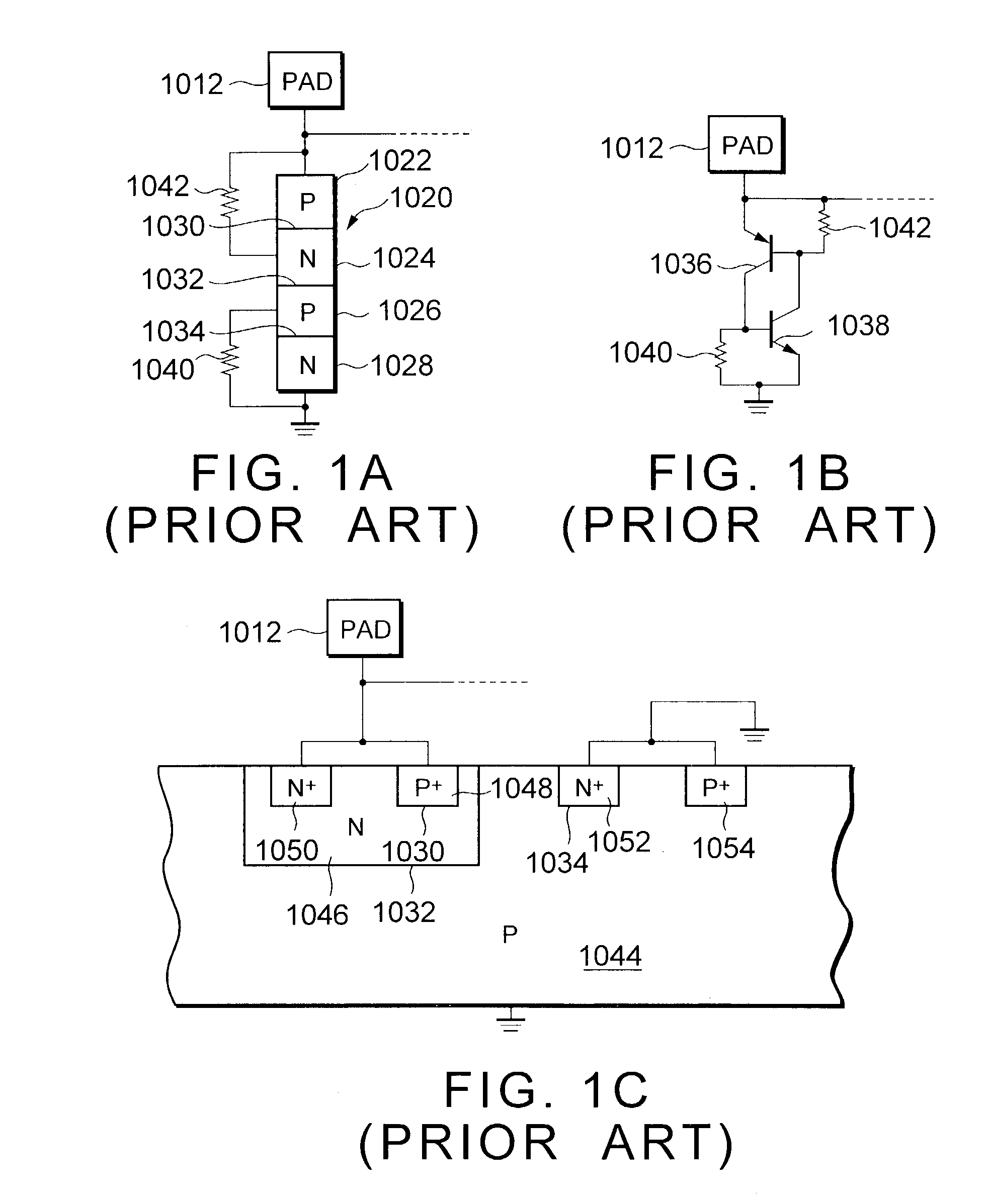
[0306]A protecting operation when surge current is applied to the external connection electrode not shown connected thereto the ESD protection device 9 of the present embodiment via the first trigger device 15, fundamentally, similar to a case of the ESD protection device 7 of the seventh embodiment, therefore detailed explanation will be omitted. Meanwhile, in the ESD protection device 9 of the present embodiment, the first N diffusion region 221 and the second P diffusion region 123 are arranged such that respective boundaries opposing to each other constitute irregularity shapes and being brought in mesh with each other, therefore, an impedance of current passage at the time of protective operation that is SCR operation can be further lowered or on condition of the same impedance value, an area of the ESD protection device can be further decreased.

[0307]Next, a ninth embodiment of an ESD protection device of the present invention will be explained. FIG. 14A is a view for explaini...

tenth embodiment

[0347]Now, a first modified example of an ESD protection device of the present invention improve above-mentioned problems. Referring FIG. 22, a first modified example is explained as following.

[0348]As shown in FIG. 22, a first modified example of a tenth embodiment of an ESD protection device of the present invention comprises a first P well region 2101, second P diffusion regions 2123 (an anode electrode), a third P diffusion region 2125 (a trigger tap electrode), N conductive type third N wells 2201 peripheries thereof being respectively surrounded by a first P well region 2001, first N diffusion regions 2221, and a second N diffusion region (a cathode electrode) 2223 and all are formed on a P type substrate (not shown).

[0349]Furthemor the first modified example of a tenth embodiment of an ESD protection device of the present invention comprises a substrate control electrode and a N-well electrode for control of substrate, which are alternately located like comb-shape so as to ma...


PUM


Abstract

There is provided an electrostatic discharge protection device comprising a P conductive type first P well region 101 formed in a P type epitaxial layer 31 being deposited on a surface of a P+ substrate 30 having a prescribed thickness, an N conductive type first N well 101 a periphery thereof being brought into direct contact with and surrounded by a first P well region 101, P conductive type first P diffusion regions 121a and 121b, a P conductive type third P diffusion region 125, and an N conductive type second N diffusion region 223 arranged within a first P well region 101, and a P conductive type second P diffusion region 123 and an N conductive type first N diffusion region 221 arranged within a first N well 201.

Description

BACKGROUND OF THE INVENTION[0001]1. Field of the Invention[0002]The present invention relates to an electrostatic discharge protection device of a semiconductor device (hereinafter, referred to as LSI), more particularly to an electrostatic discharge protection device which is formed in an LSI chip, and performs as a Silicon Controlled Rectifier (SCR) type operation when respective circuit devices in the LSI are protected from electrostatic discharge.[0003]2. Description of the Prior Art[0004]Recently, a function of an LSI has been complicated, moreover, its packaging density has been formed into high density. Further, during the fabricating process, assembling process, and others of the LSI, the LSI is liable to be easily broken because of ESD (electrostatic discharge). Therefore, an electrostatic discharge protection device (hereinafter, referred to as ESD protection device) has been used for protecting circuit devices from ESD by discharging static electricity efficiently and wit...

Claims


Application Information

Patent Timeline
IPC IPC(8): H01L29/74H01L27/02H02H9/00
CPCH01L27/0262
Inventor KODAMA, NORIYUKI
Owner RENESAS ELECTRONICS CORP
Why Eureka
Try Eureka