Method and apparatus for standby power reduction in semiconductor devices

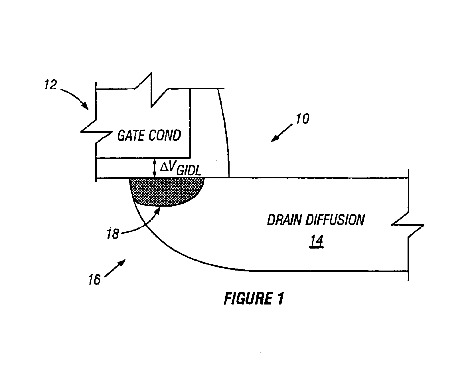
a technology of semiconductor devices and standby power, applied in the field of semiconductor devices, can solve the problems of constant current leakage through thin dielectric layers, gidl present an ongoing challenge to circuit designers, and the gate overlying the diffusion region or draining the diffusion region to at least some extent is susceptible to gidl, so as to reduce the voltage supplied, prevent the voltage on the local power supply node, and reduce the effect of voltag

Inactive Publication Date: 2005-03-29
MICRON TECH INC
View PDF23 Cites 18 Cited by
  • Summary
  • Abstract
  • Description
  • Claims
  • Application Information

AI Technical Summary

Benefits of technology

In accordance with one aspect of the invention, a local power supply node in a semiconductor device is selectively coupled to a supply potential by means of one or more decoupling transistors. The decoupling transistor(s) is / are controlled by means of one or more control signals to interrupt the direct coupling of the local power supply node to the supply potential only during selected operational events, thereby locally reducing the voltage supplied to elements susceptible to GIDL.
In accordance with another aspect of the invention, a “global” power supply signal (i.e., a signal provided to various functional elements throughout an integrated circuit), is coupled to a local power supply node by means of one or more decoupling transistors, as well as by a vt-connected transistor. When the one or more decoupling transistors are off, the voltage on the local power supply node is prevented from exceeding approximately one transistor threshold voltage (vt; approximately 0.6- to 0.7-volts) less than the global power supply signal level. The reduced voltage on the local power supply node lessens the GIDL current in the GIDL-susceptible elements, including P-channel transistors, coupled the local power supply node.

Problems solved by technology

In the field of semiconductor fabrication, a persistent issue has been that of current leakage through thin dielectric layers.
It is believed that any transistor having a gate overlying source or drain diffusion region to at least some extent is susceptible to GIDL.
As gate dielectrics, which are typically formed of silicon oxide, become increasingly thinner due to continued scaling of semiconductor structures in pursuit of faster and more efficient operation, problems relating to GIDL present an ongoing challenge to circuit designers.
Such carrier generation tends to impair device performance.
In addition to increasing standby power, in the context of dynamic random access memory devices, GIDL can degrade data retention time, such that the maximum time between refreshes of a memory array is undesirably decreased.
Among other considerations, the various proposed strategies for alleviating GIDL phenomenon in semiconductor devices often suffer to greater or lesser extents from the disadvantages of unduly increasing device size, adding complexity to the fabrication process, or degrading device performance.

Method used


Image

  • Method and apparatus for standby power reduction in semiconductor devices
  • Method and apparatus for standby power reduction in semiconductor devices
  • Method and apparatus for standby power reduction in semiconductor devices

Examples


Embodiment Construction

In the disclosure that follows, in the interest of clarity, not all features of actual implementations are described. It will of course be appreciated that in the development of any such actual implementation, as in any such project, numerous engineering and programming decisions must be made to achieve the developers' specific goals and subgoals (e.g., compliance with system and technical constraints), which will vary from one implementation to another. Moreover, attention will necessarily be paid to proper engineering practices for the environment in question. It will be appreciated that such a development effort might be complex and time-consuming, but would nevertheless be a routine undertaking for those of ordinary skill in the relevant fields.

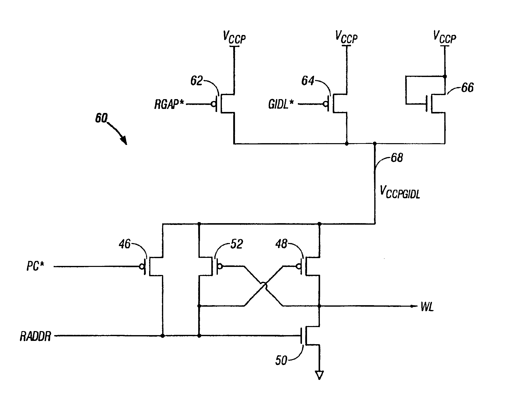
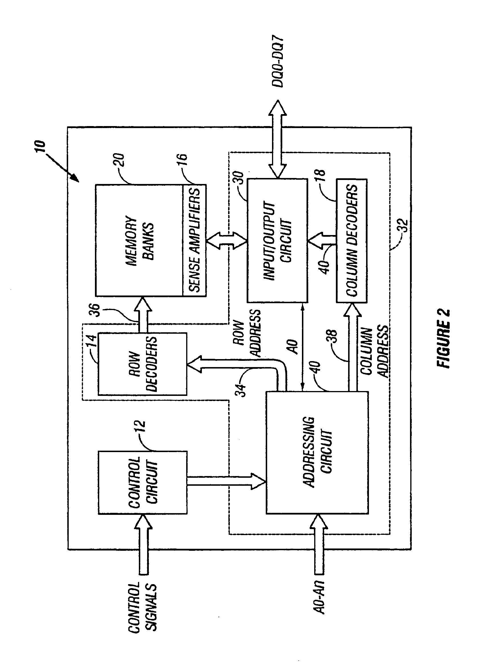
Referring to FIG. 2, there is shown a highly simplified schematic / block diagram of a semiconductor memory device 10 in accordance with one embodiment of the invention. In the disclosed embodiment, memory device 10 is a dynamic random acce...


PUM


Abstract

A word line driver circuit for a semiconductor memory device. One or more transistors in the driver circuit are fabricated such that they are susceptible, under certain conditions, to gate-induced diode leakage (GIDL). One terminal of the transistors are coupled to a local supply node, which during standby conditions when the word line driver circuit is not driving a word line, is maintained at a voltage less than that of a global power supply node. In one embodiment, the local power supply node is coupled to the global power supply node by means of at least one decoupling transistor receiving a control signal at its gate and by a vt-connected transistor, such that the voltage on the local power supply node is maintained at a level not exceeding one transistor threshold voltage less than the global power supply node voltage when the decoupling transistor is off. When the decoupling transistor(s) is / are switched on prior to word line driving operation, the voltage on the local power supply node rises to the voltage of the global power supply node. Preferably, the control signal(s) controlling the decoupling transistor(s) are, or are derived from, control signals generated for purposes other than controlling the decoupling transistor.

Description

FIELD OF THE INVENTIONThis invention relates generally to semiconductor devices, and more particularly relates to methods and apparatuses for reducing power consumption of semiconductor devices.BACKGROUND OF THE INVENTIONThe field of semiconductor memory devices generally and complementary metal-oxide semiconductor (CMOS) devices in particular is enormously active and rapidly developing. Various categories and sub-categories of semiconductor devices are known and commercially available. The ever-increasing popularity and ubiquity of computers and computer-based devices, both in the consumer and industrial realms, is such that the demand for semiconductor memory devices of a variety of different types will continue to grow for the foreseeable future.In the field of semiconductor fabrication, a persistent issue has been that of current leakage through thin dielectric layers. Those of ordinary skill in the art will appreciate that leakage through the gate dielectrics of field-effect tr...

Claims


Application Information

Patent Timeline
Patent Type & Authority Patents(United States)
IPC IPC(8): G11C11/408G11C8/00G11C8/08
CPCG11C8/08G11C11/4085G11C2207/2227
Inventor KOELLING, JEFFSCHRECK, JOHNMORRIS, JONOMER, RISHAD
Owner MICRON TECH INC
Why Eureka
Try Eureka