
Structure and method for electrical isolation of optoelectronic integrated circuits

a technology of optoelectronic integrated circuits and integrated circuits, which is applied in the direction of optical elements, semiconductor lasers, instruments, etc., can solve the problems of degrading the mechanical integrity of the device, affecting the electrical isolation of the device, so as to achieve the effect of facilitating further processing steps and maintaining good mechanical integrity and thermal conductivity

Inactive Publication Date: 2007-03-27
MAJANDRO LLC
View PDF11 Cites 0 Cited by
  • Summary
  • Abstract
  • Description
  • Claims
  • Application Information

AI Technical Summary

Benefits of technology

"The patent describes a method of oxidizing layers in semiconductor devices using etched cavities instead of mesas that expose the sidewalls of the layers. This approach results in planar structures that allow for easier processing steps and maintain good mechanical integrity and thermal conductivity. The oxidized region can be shaped and sized by the shape of the cavity and the placement of other cavities, and can be used for various applications such as optical waveguiding, electrical conduction, and thermal isolation."

Problems solved by technology

This method leads to a high level of wafer non-planarity that complicates subsequent processing steps.
Moreover, the large amount of materials removed degrade the device's mechanical integrity and increases its thermal resistance.
The problem is especially severe in devices like vertical-cavity surface-emitting lasers, where the oxidation layer is usually embedded far beneath the wafer surface.

Method used


Image

  • Structure and method for electrical isolation of optoelectronic integrated circuits
  • Structure and method for electrical isolation of optoelectronic integrated circuits
  • Structure and method for electrical isolation of optoelectronic integrated circuits

Examples


Embodiment Construction

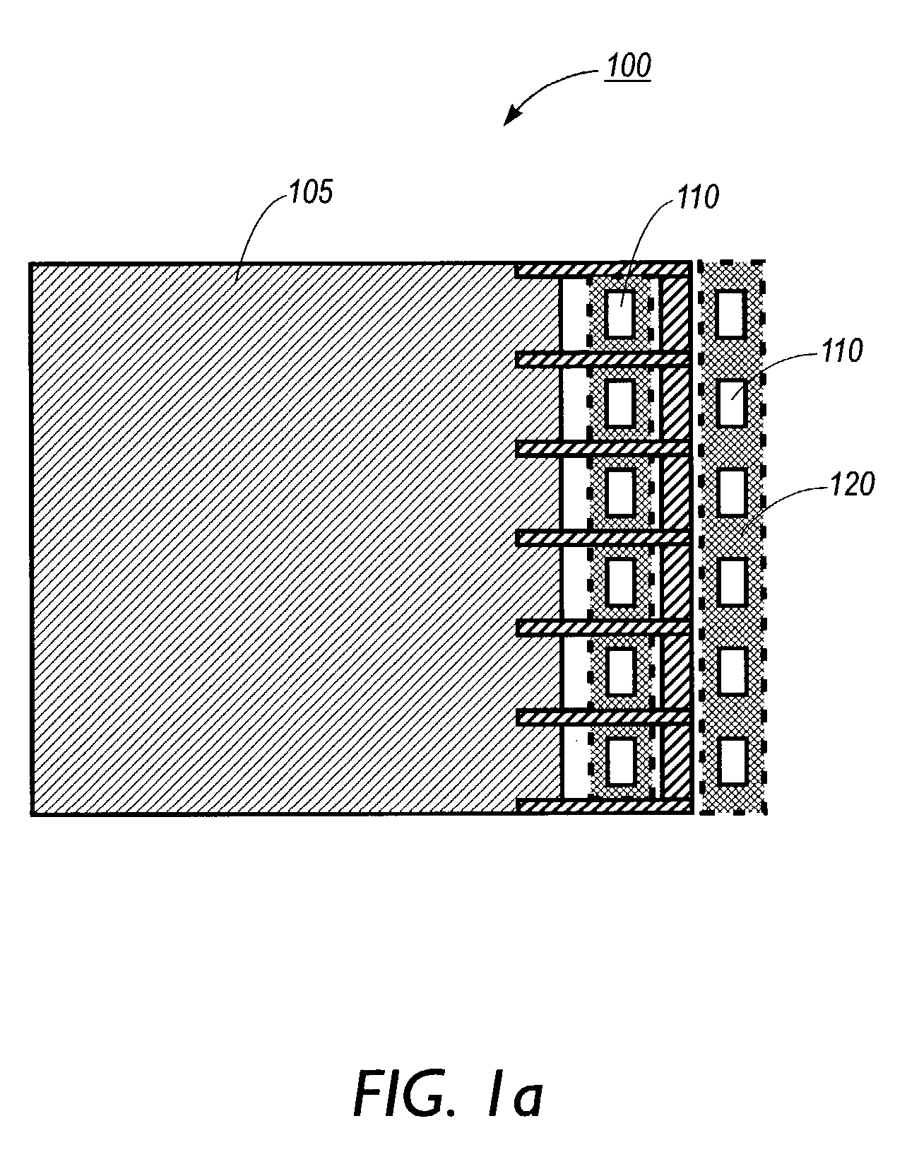
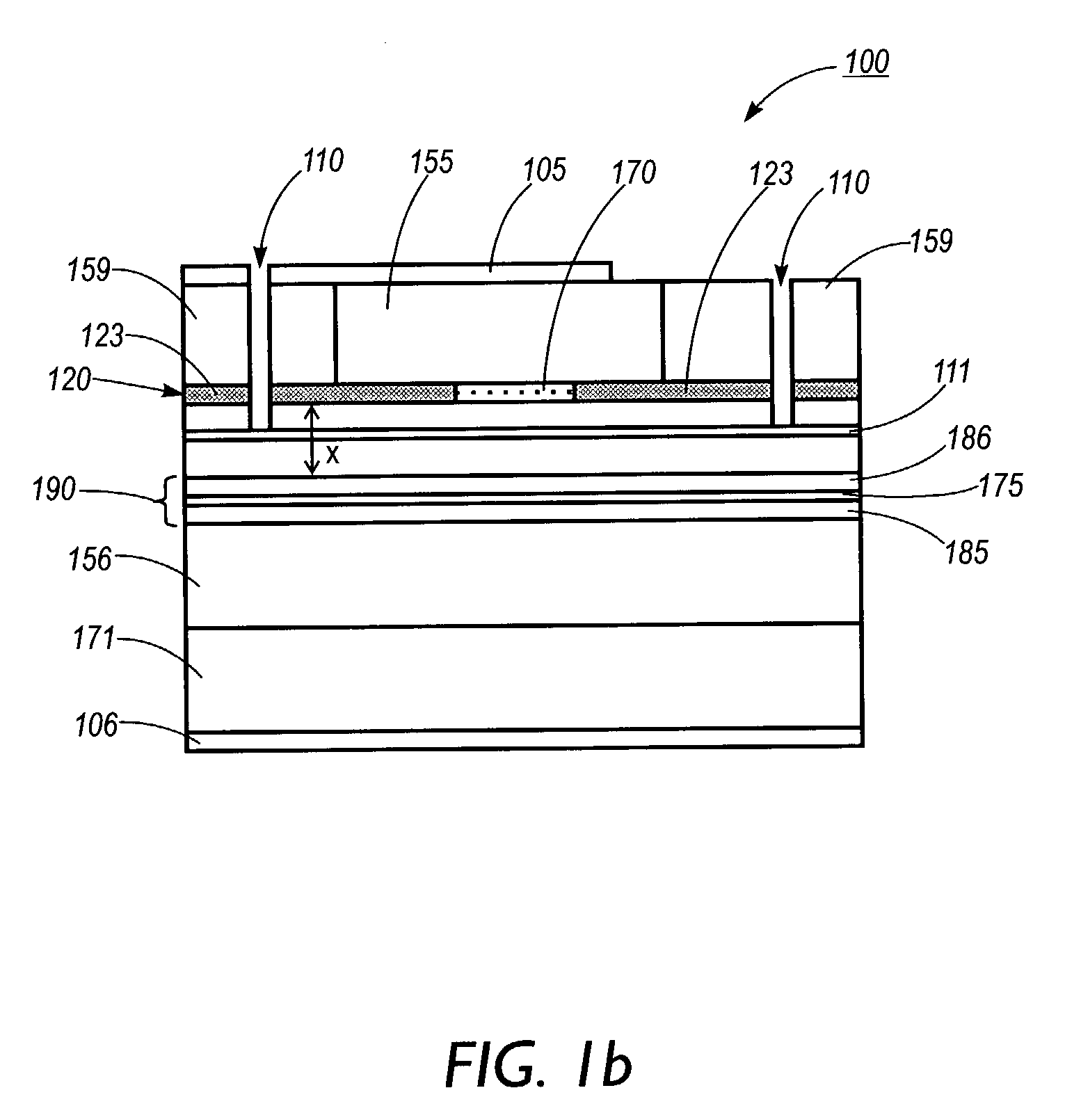
[0030]An embodiment in accordance with the invention, edge emitting laser structure 100 is shown in FIG. 1a in top view and in FIG. 1b in cross section. Ga0.4In0.6P quantum well active layer 175, typically about 80 Å thick, is bordered by p-type (Al0.6Ga0.4)0.5In0.5P barrier layer 186 and by n-type (Al0.6Ga0.4)0.5In0.5P barrier layer 185, both barrier layers 185 and 186 typically being about 0.12 μm thick. Etched cavities 110 allow access to AlyGa1-yAs buried layer 120 for lateral oxidation. The value selected for y is generally greater than 0.95 and a typical value is 0.99. Al0.99Ga1.01As buried layer 120 is typically less than 1000 Å thick. Stripe 170 of Al0.99Ga0.01As buried layer 120 remains unoxidized to provide a lateral index of refraction step while regions 123 are oxidized to define stripe 170. GaInP layer 111 is optional and lies below Al0.99Ga0.01As buried layer 120 and serves as an etch stop for etching of cavities 110. P type Al0.5In0.5P cladding layer 155 overlies Al0....


PUM


Abstract

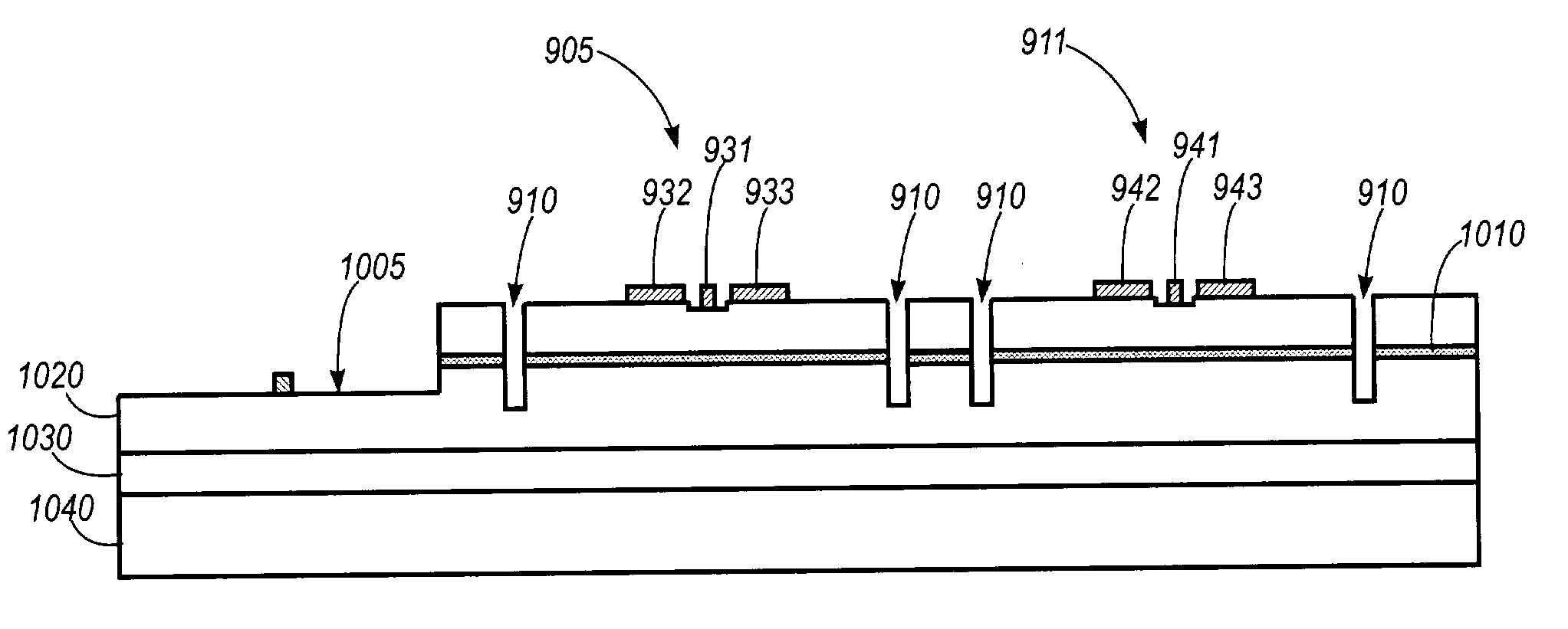
Semiconductor devices in an optoelectronic integrated circuit are electrically isolated from each other by using planar lateral oxidation to oxidize a buried semiconductor layer vertically separating the semiconductor devices.

Description

CROSS-REFERENCE TO RELATED APPLICATIONS[0001]This is a divisional of application Ser. No. 09 / 473,109; filed Dec. 27, 1999 now U.S. Pat. No. 6,545,335.BACKGROUND OF INVENTION[0002]In a variety of semiconductor applications it is desirable to access buried semiconductor layers in order to oxidize the buried layer. Numerous photonic, electronic and micro-mechanical devices require a region of buried material that is electrically insulating or differs from surrounding material by having a lower refractive index. Such a material can be formed during device fabrication by selectively converting one or more buried semiconductor layers into an electrically insulating low refractive index native oxide.[0003]An oxidized region may be made to partially or completely surround a region of interest to produce a desired optical effect due to the lower refractive index of the oxide region. Buried oxide layers may also function to electrically isolate different regions of a device or to electrically...

Claims


Application Information

Patent Timeline
Patent Type & Authority Patents(United States)
IPC IPC(8): H01L21/00G02B6/122G02B6/13H01L27/15H01S5/026H01S5/183H01S5/22
CPCH01S5/0261H01S5/18388H01S5/1833H01S5/18313
Inventor CHUA, CHRISTOPHER L.FLOYD, PHILIP D.PAOLI, THOMAS L.SUN, DECAI
Owner MAJANDRO LLC
Learn More