Electronic device

a technology of electronic devices and components, applied in the field of electronic devices, can solve the problems of only reaching the operating temperature briefly, and achieve the effects of low electrical contact resistance, efficient thermal coupling, and compact output stage design

Inactive Publication Date: 2007-04-03
SCHAEFFLER TECH AG & CO KG
View PDF3 Cites 6 Cited by
  • Summary
  • Abstract
  • Description
  • Claims
  • Application Information

AI Technical Summary

Benefits of technology

[0005]An object of the present invention is, therefore, to devise an electronic device of the type mentioned at the outset that will render possible a low ohmic contact resistance between the conductor part and the semiconductor chip and an efficient transfer of heat from the semiconductor chip to the conductor part. Moreover, it is also intended for the electronic device to exhibit a good long-term stability with respect to resisting the temperature fluctuations occurring on the semiconductor chip during normal use.

Problems solved by technology

However, it is also possible that the operating temperature is reached only briefly, for example during the occurrence of a peak load.

Method used


Image

  • Electronic device
  • Electronic device
  • Electronic device

Examples


Embodiment Construction

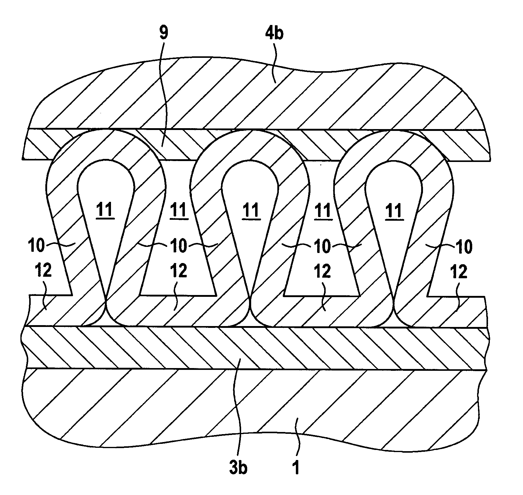
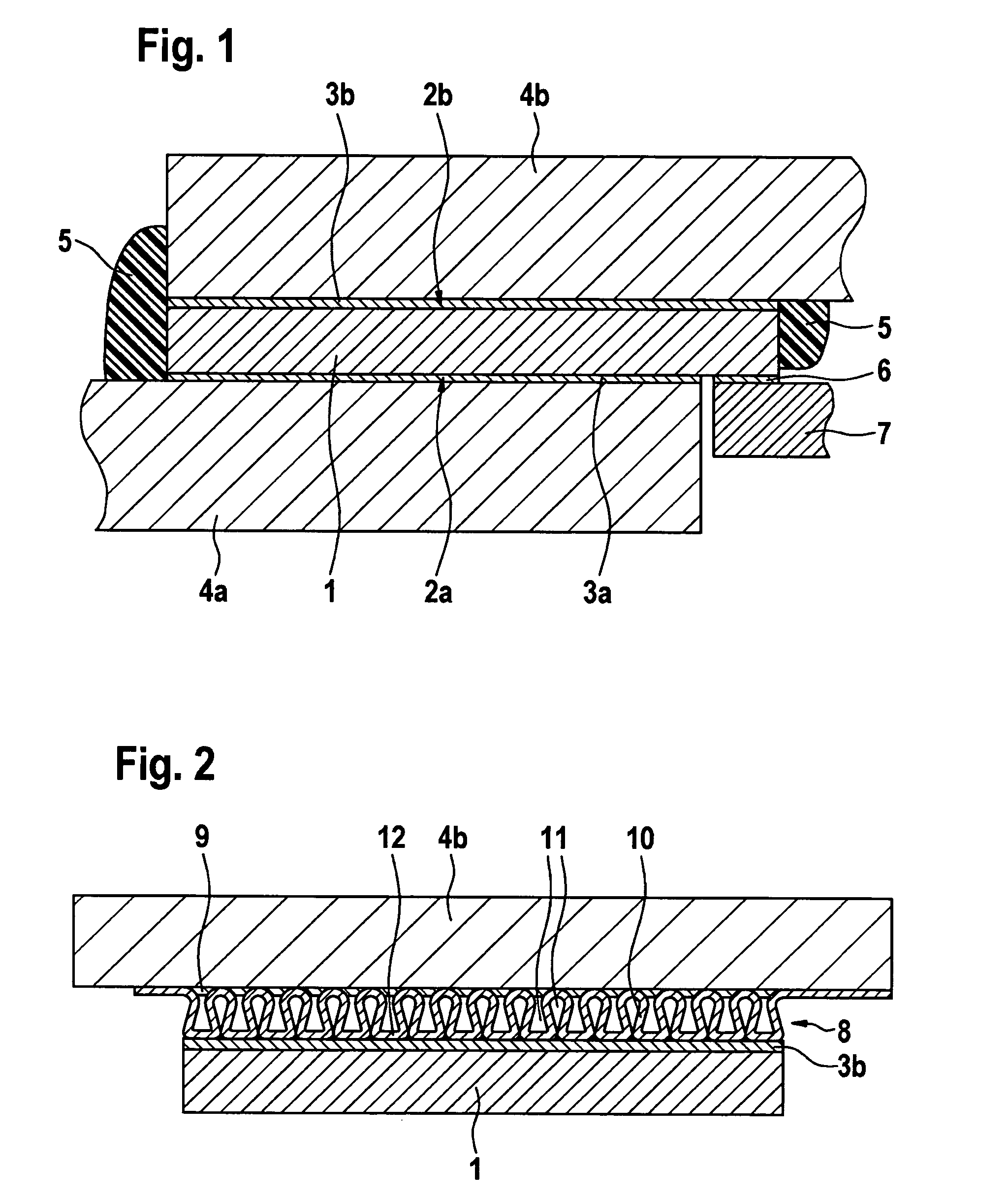
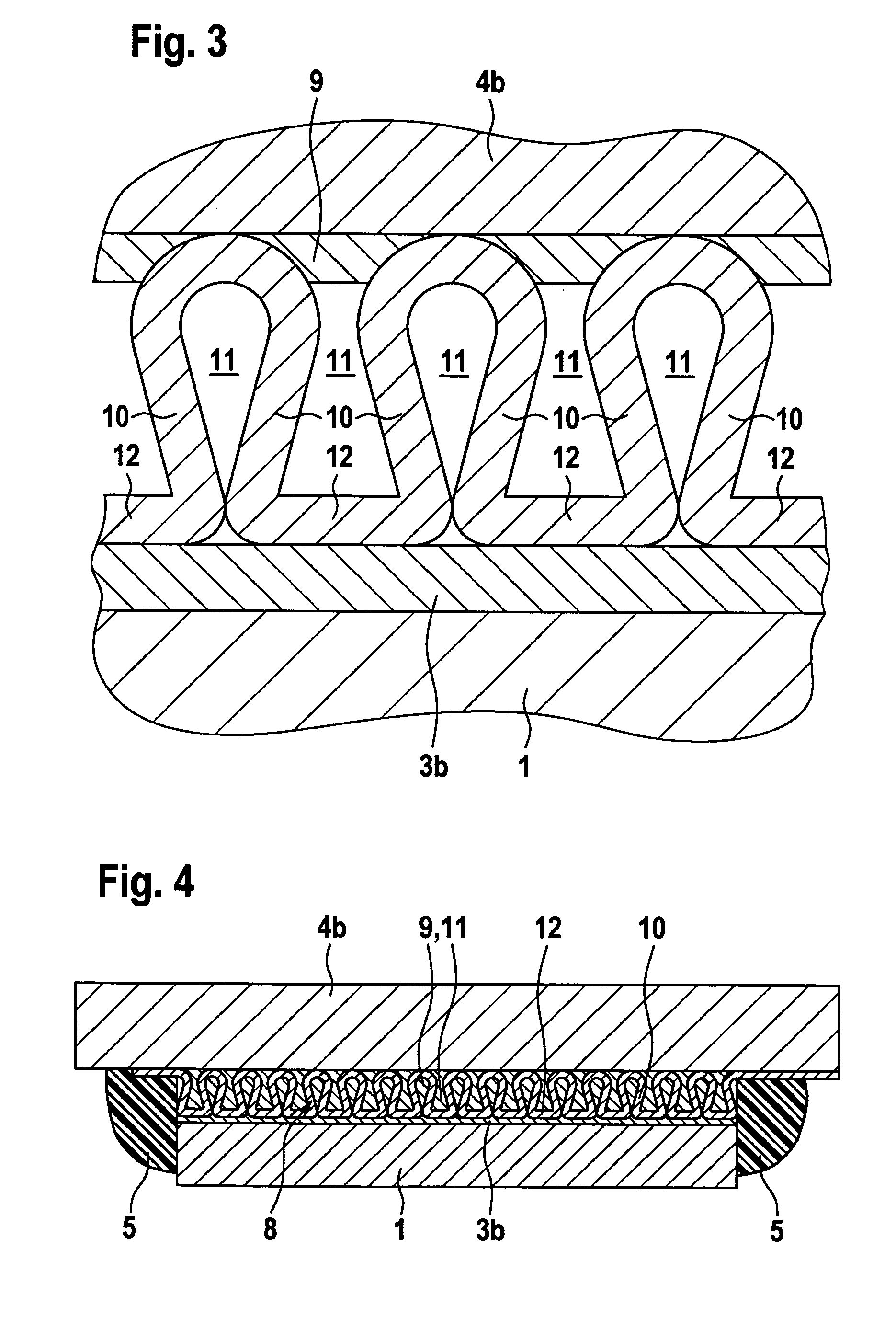
[0030]An electronic device, namely an output stage for driving the winding of a brushless electromotor, has a plurality of semiconductor chips 1 designed as power transistors, which in a manner known per se form a bridge circuit having a plurality of interconnected half-bridges.

[0031]In the exemplary embodiment shown in FIG. 1, the mutually opposing flat sides of semiconductor chip 1 are each formed as contact sides 2a, 2b. A first contact side 2a is electroconductively surface-bonded via a first soldering-agent layer 3a to a first metallic conductor part 4a. A second contact side 2b is electroconductively surface-bonded via a second soldering-agent layer 3b to a second metallic conductor part 4b. In this context, soldering-agent layers 3a, 3b are surface-bonded, with their one flat side to the facing contact side 2a, 2b, of semiconductor chip 1 and, with their opposing other flat side to the corresponding conductor part 4a, 4b. Conductor parts 4a, 4b are designed as massive conduct...


PUM


Abstract

An electronic device has at least one semiconductor chip, which has mutually opposing contact sides, of which one first contact side is electroconductively surface-bonded via a first, solid soldering-agent layer to at least one first metallic conductor part. The semiconductor chip is electroconductively surface-bonded on its second contact side facing opposite the first contact side via a second soldering-agent layer to at least one second metallic conductor part. The softening temperature of the second soldering-agent layer is adapted to an operating temperature that occurs in this soldering-agent layer during operation of the device in such a way that the second soldering-agent layer is doughy or liquid at the operating temperature. The second soldering-agent layer is laterally bounded by a flow-off protection device.

Description

[0001]Priority is claimed to German Patent Application No. DE 103 49 444.8, filed on Oct. 23, 2003, the entire disclosure of which is incorporated by reference herein.[0002]The present invention is directed to an electronic device having at least one semiconductor chip, which has mutually opposing contact sides, of which one first contact side is electroconductively surface-bonded via a first, solid soldering-agent layer to at least one first metallic conductor part. The present invention is also directed to an electronic device having at least one semiconductor chip which is electroconductively surface-bonded on one contact side via at least one solid soldering-agent layer to at least one metallic conductor part.BACKGROUND[0003]An electronic device of this kind, designed as an output stage for driving a brushless electromotor, is known in the field. As semiconductor chips, the device has a plurality of transistors which are mounted on a printed-circuit board. On their front and bac...

Claims


Application Information

Patent Timeline
Patent Type & Authority Patents(United States)
IPC IPC(8): H01L23/48H01L21/60H01L23/00H01L23/02H01L23/31H01L23/482H01L23/488H01L25/07H05K1/18H05K7/20
CPCH01L23/3185H01L23/482H01L23/562H01L24/32H01L24/33H01L24/83H01L2924/13055H01L2224/83801H01L2924/01013H01L2924/01029H01L2924/19043H01L2924/01006H01L2924/01033H01L2924/014H01L2924/00H01L2924/00011H01L2224/2612H01L2224/83205
Inventor HILL, WOLFGANG
Owner SCHAEFFLER TECH AG & CO KG
Why Eureka
Try Eureka