
Organic electroluminescence element

Inactive Publication Date: 2007-04-10
SANYO ELECTRIC CO LTD
View PDF16 Cites 9 Cited by
  • Summary
  • Abstract
  • Description
  • Claims
  • Application Information

AI Technical Summary

Benefits of technology

[0017]An object of the present invention is to provide an organic electroluminescence element capable of obtaining high luminance and high luminous efficiency.

Problems solved by technology

Thus, if the electron transport layer or the luminescent layer is formed with single employment of the compound having the carbazole group or its derivative, or if such a compound or its derivative is employed for the electron transport layer or the luminescent layer as a host material of a doping method, it results in very lower durability and lower luminous efficiency.

Method used


Image

  • Organic electroluminescence element
  • Organic electroluminescence element
  • Organic electroluminescence element

Examples


##ventive example 1

Inventive Example 1

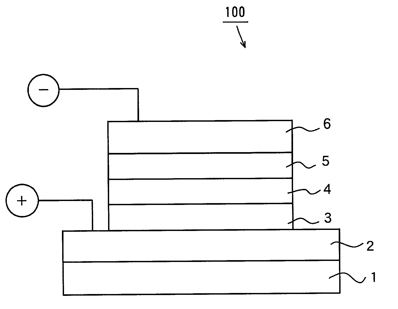
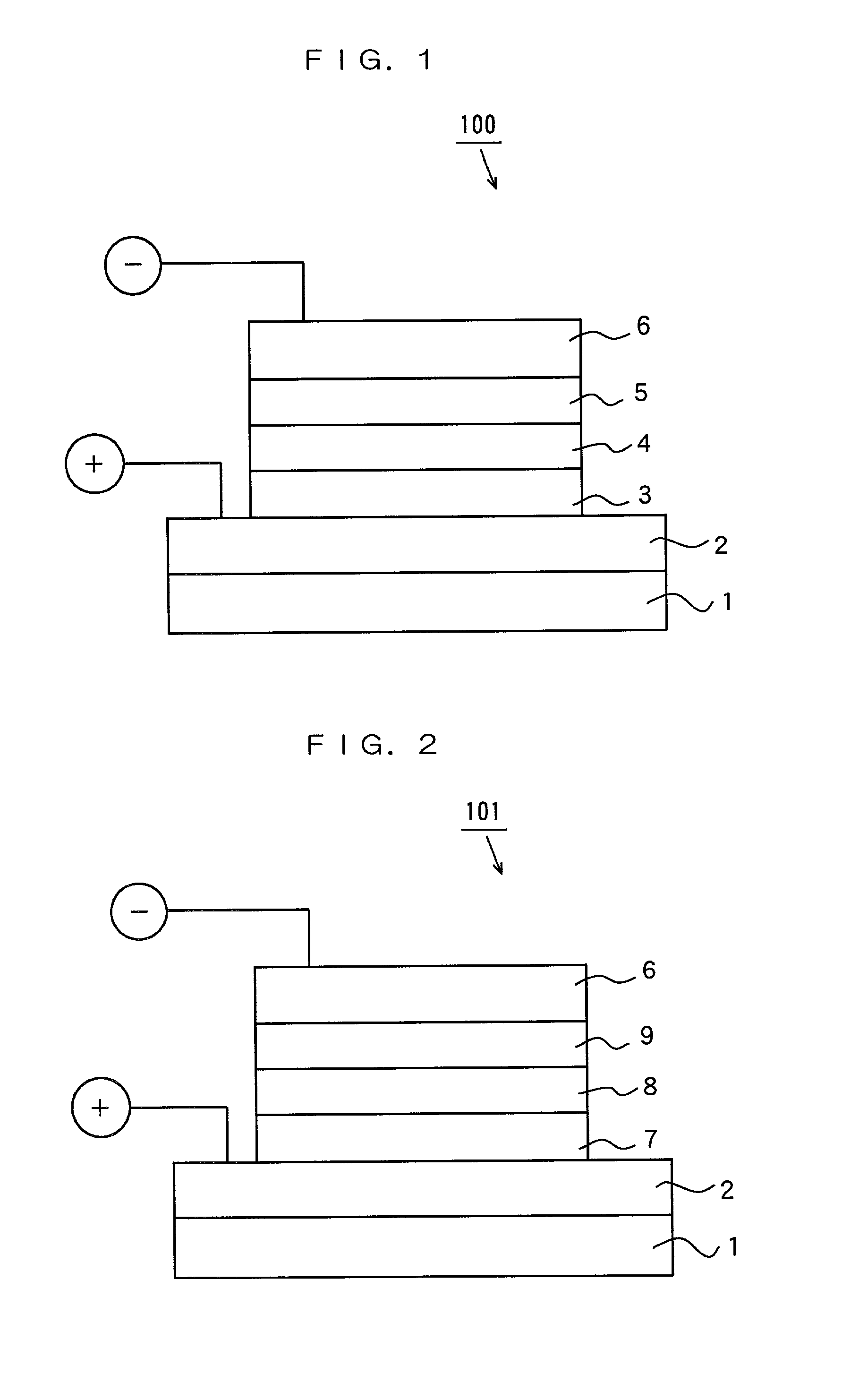
[0082]An organic El element in the inventive example 1 has such a structure as shown in FIG. 1. A hole injection electrode (anode) 2 is composed of indium-tin oxides (ITO). A hole transport layer 3 has a thickness of 500 Å and is composed of 2TNATA having a molecular structure of a chemical formula (14) shown below. A luminescent layer 4 having a thickness of 150 Å contains NPB having a molecular structure of a chemical formula (15) as a host material and also contains as a luminescent dopant 5% by weight of Rubrene for the host material. An electron transport layer 5 having a thickness of 350 Å contains Alq as an electron trasport material (host material) and also contains as a carrier transportable dopant 4% by weight of CBP for the electron transport material. An electron injection electrode (cathode) 6 is composed of a MgIn alloy (a ratio of 10 to 1) with a thickness of 2000 Å.

[0083]

[0084]The organic EL element having the above described structure was manufact...

##ventive example 2

Inventive Example 2

[0087]An organic EL element in the inventive example 2 was manufactured under the same conditions as applied to the organic EL element in the inventive example 1 except that TCTA was substituted for CBP as the carrier transportable dopant to be employed for the electron transport layer 5.

##ventive example 3

Inventive Example 3

[0088]An organic EL element in the inventive example 3 was manufactured under the same conditions as applied to the organic EL element in the inventive example 1 except that AZB was substituted for CBP as the carrier transportable dopant to be employed for the electron transport layer 5.


PUM

PropertyMeasurementUnit
Percent by massaaaaaaaaaa
Weightaaaaaaaaaa

Abstract

An electron transport layer includes an electron transport material (host material) and a carrier transportable dopant. The carrier transportable dopant is contained 1% by weight to 50% by weight, preferably 1% by weight to 10% by weight for the electron transport material. A compound having a carbazole group or a derivative of the compound is employed as the carrier transportable dopant. A complex of an 8-hydroxyquinoline derivative and metal is employed as the electron transport material.

Description

BACKGROUND OF THE INVENTION[0001]1. Field of the Invention[0002]The present invention relates to an organic electroluminescence element.[0003]2. Description of the Background Art[0004]An organic electroluminescence element (hereinafter referred to as an organic EL element) is expected as a new self-light emission type element. The organic EL element has such a stacked structure that a carrier transport layer (an electron transport layer or a hole transport layer) and a luminescent layer are formed between a hole injection electrode and an electron injection electrode.[0005]An electrode material which has a large work function such as gold or ITO (indium-tin oxides) is employed for the hole injection electrode, while a material which has a small work function such as Mg (magnesium) or Li (lithium) is employed for the electron injection electrode.[0006]Organic materials are employed for a hole transport layer, a luminescent layer and an electron transport layer. Materials which have t...

Claims


Application Information

Patent Timeline
IPC IPC(8): H05B33/12H01L27/32H01L51/50C09K11/06H01L51/00H01L51/30H05B33/18
CPCH01L51/002H01L51/0061H01L51/0072H01L51/5012H01L51/0054H01L51/006H01L51/0065H01L51/0077H01L51/0081Y10S428/917H10K71/30H10K85/622H10K85/653H10K85/636H10K85/633H10K85/30H10K85/324H10K85/6572H10K50/11
Inventor HAMADA, YUJI
Owner SANYO ELECTRIC CO LTD
Features
  • Generate Ideas
  • Intellectual Property
  • Life Sciences
  • Materials
  • Tech Scout
  • Unparalleled Data Quality
  • Higher Quality Content
  • 60% Fewer Hallucinations
Learn More