Method of fabricating a laser diode that includes thermally cleaning a deposition reactor using a gas mixture of arsine and hydrogen

a laser diode and deposition reactor technology, applied in lasers, semiconductor devices, semiconductor lasers, etc., can solve the problems of additional apparatus to increase costs, adversely affect the optical characteristics of ingaasn qw layers, and deterioration of optical characteristics of ingaasn qw layers, so as to improve the optical characteristics of ingaasn quantum wells

Active Publication Date: 2007-04-10
SAMSUNG ELECTRONICS CO LTD
View PDF4 Cites 0 Cited by
  • Summary
  • Abstract
  • Description
  • Claims
  • Application Information

AI Technical Summary

Benefits of technology

[0020]The present invention provides a method of fabricating a laser diode, which can improve the optical characteristics of an InGaAsN quantum well (QW) layer. In this method, a process of forming an Al-containing semiconductor material layer and a process of forming the InGaAsN QW layer can be performed in a single deposition reactor.

Problems solved by technology

However, a recent paper describes that the optical characteristics of an InGaAsN QW layer are deteriorated due to the influence of Al (refer to Jpn. J. Appl. Phys., Vol. 43, No. 4A, 2004, pp.
Al may adversely affect the optical characteristics of an InGaAsN QW layer particularly when a process of forming a semiconductor material layer, such as an AlGaAs clad layer or a distributed brag reflection (DBR) layer, and a process of forming the InGaAsN QW layer on the semiconductor material layer are performed in a single deposition reactor.
However, this method requires an additional apparatus to increase cost and reduces process speed to lower efficiency.
Further, since a layer forming process is stopped and then resumed, a semiconductor material layer may have defects or be contaminated with impurities, thus degrading the reproducibility or reliability of laser diodes.

Method used


Image

  • Method of fabricating a laser diode that includes thermally cleaning a deposition reactor using a gas mixture of arsine and hydrogen
  • Method of fabricating a laser diode that includes thermally cleaning a deposition reactor using a gas mixture of arsine and hydrogen
  • Method of fabricating a laser diode that includes thermally cleaning a deposition reactor using a gas mixture of arsine and hydrogen

Examples


Embodiment Construction

[0027]The present invention will now be described more fully with reference to the accompanying drawings, in which exemplary embodiments of the invention are shown.

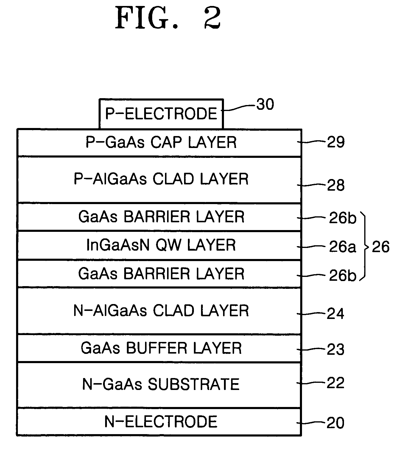
[0028]FIGS. 2 and 3 are cross-sectional views of laser diodes formed according to the present invention.

[0029]Referring to FIG. 2, a laser diode includes a GaAs buffer layer 23, an n-type AlGaAs clad layer 24, an active layer 26, a p-type AlGaAs clad layer 28, and a p-type GaAs cap layer, which are sequentially stacked on an n-type GaAs substrate 22.

[0030]An n-type electrode 20 is disposed under the n-type GaAs substrate 22, and a p-type electrode 30 is disposed on the p-type GaAs cap layer.

[0031]Also, the active layer 26 includes an InGaAsN quantum well (QW) layer 26a and GaAs barrier layers 26b disposed between the InGaAsN QW layer 26a and the n-type and p-type AlGaAs clad layers 24 and 28, respectively.

[0032]Referring to FIG. 3, a laser diode includes a GaAs buffer layer 43, a lower distributed brag reflection (DBR) la...


PUM

PropertyMeasurementUnit
temperatureaaaaaaaaaa
wavelength rangeaaaaaaaaaa

Abstract

Provided is a method of fabricating a laser diode including a lower Al-containing semiconductor material layer, a active layer, and an upper Al-containing semiconductor material layer. The method includes thermally cleaning the inside of a deposition reactor in which a substrate on which the lower Al-containing semiconductor material layer is stacked is loaded. During the thermal cleaning process, the inside of the deposition reactor is thermally treated at a predetermined temperature in an atmosphere of a gas mixture of AsH3 and H2 that is injected into the deposition reactor.

Description

BACKGROUND OF THE INVENTION[0001]This application claims the priority of Korean Patent Application No. 2004-50480, filed on Jun. 30, 2004 in the Korean Intellectual Property Office, the disclosure of which is incorporated herein in its entirety by reference.[0002]1. Field of the Invention[0003]The present invention relates to a method of fabricating a laser diode, and more particularly, to a method of fabricating a laser diode, which can improve the optical characteristics of an InGaAsN quantum well (QW) layer.[0004]2. Description of the Related Art[0005]Nowadays, extensive research for applications of optical devices has progressed along with developments in high-speed data communications in the field of broad technologies including laser printers, optical image storage, underground optical cable systems, and optical communications.[0006]Owing to the increased demand for more rapid and economical communication systems, optical fibers having broad transmission bands in a longer wave...

Claims


Application Information

Patent Timeline
Patent Type & Authority Patents(United States)
IPC IPC(8): H01L21/00H01S5/00H01S5/183H01S5/343
CPCB82Y20/00H01S5/34306H01S5/0014H01S5/183H01S2304/04Y10S438/905H01S5/34
Inventor KIM, KI-SUNGPARK, YONG-JO
Owner SAMSUNG ELECTRONICS CO LTD
Why Eureka
Try Eureka